Manufacturing methods of display base plate and display panel

A manufacturing method and array substrate technology, applied in nonlinear optics, instruments, optics, etc., can solve problems such as crosstalk and excessive leakage current, and achieve the effects of preventing crosstalk, reducing leakage current, and improving user experience

Active Publication Date: 2015-06-03
HEFEI BOE OPTOELECTRONICS TECH +1
View PDF7 Cites 12 Cited by
  • Summary
  • Abstract
  • Description
  • Claims
  • Application Information

AI Technical Summary

Problems solved by technology

[0005] Embodiments of the present invention provide a method for manufacturing a display substrate and a method for manufacturing a display panel, which are used to solve problems such as excessive leakage current and crosstalk in thin film transistors caused by photo-alignment in the prior art, and improve the display quality of the panel user experience

Method used


Image

  • Manufacturing methods of display base plate and display panel
  • Manufacturing methods of display base plate and display panel
  • Manufacturing methods of display base plate and display panel

Examples


Embodiment Construction

[0036] Embodiments of the present invention provide a method for manufacturing a display substrate and a method for manufacturing a display panel, which are used to solve the problems of excessive leakage current and crosstalk in thin film transistors caused by photo-alignment in the prior art, and improve the display quality of the panel user experience.

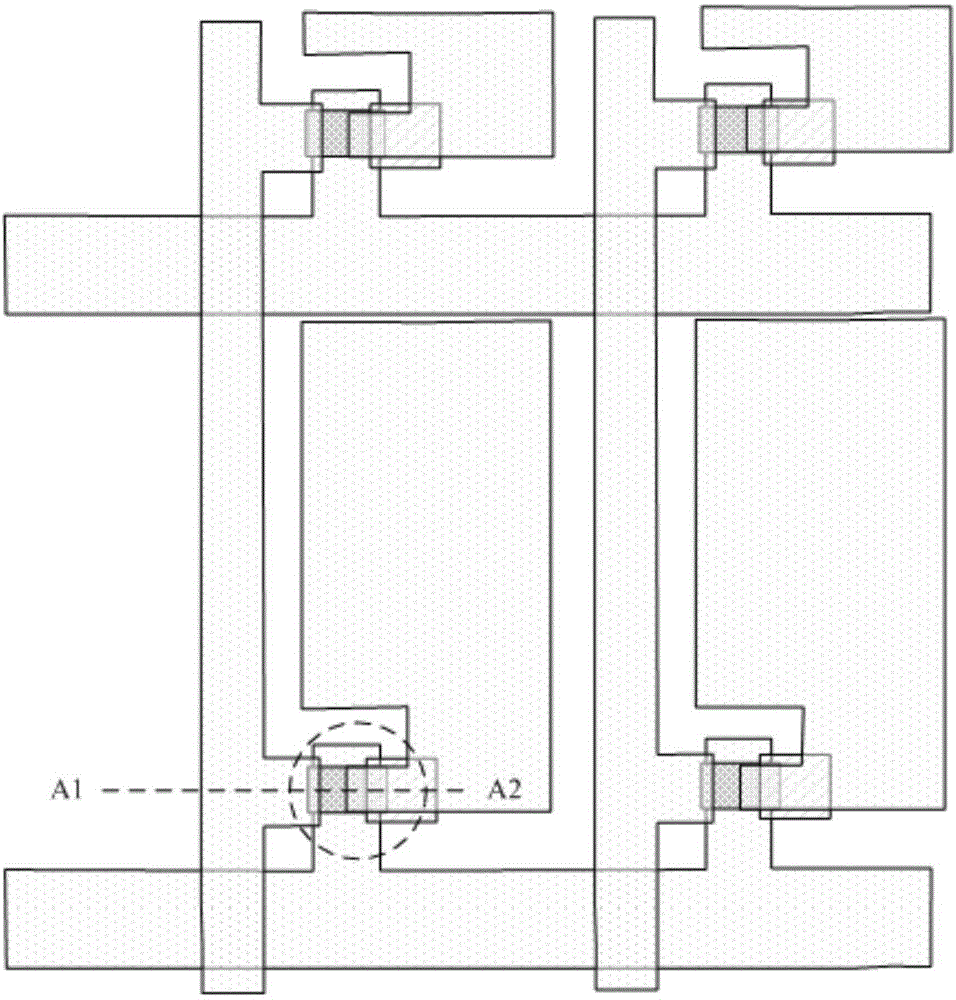
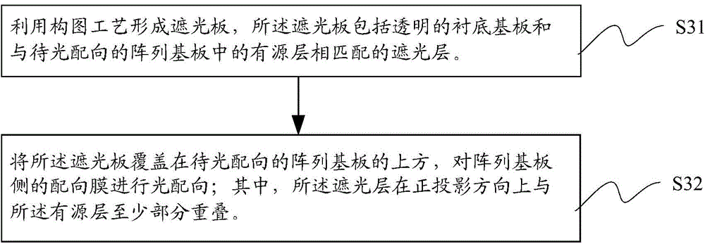
[0037] An embodiment of the present invention provides a method for manufacturing a display substrate, see image 3 , the method includes:

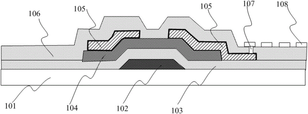
[0038] Step S31, see Figure 4 , using a patterning process to form a light-shielding plate, the light-shielding plate includes a transparent base substrate 41 and a light-shielding layer 42 matching the active layer in the array substrate to be photo-aligned.

[0039] Step S32, covering the light-shielding plate on the array substrate to be photo-aligned, and performing photo-alignment on the alignment film on the side of the array substrate; wherein, the light-shielding layer at le...


PUM

PropertyMeasurementUnit
thicknessaaaaaaaaaa
thicknessaaaaaaaaaa

Abstract

The invention discloses a manufacturing method of a display base plate and a manufacturing method of display panel, and aims at solving the problems that leakage current in a thin film transistor is too great, has crosstalk and the like, caused by optical alignment in the prior art, so that the display quality and user experience of the panel are improved. The manufacturing method of the display base plate comprises the following steps: forming a light shielding plate by using a composition process, wherein the light shielding plate comprises a transparent lining base plate and a light shielding layer which is matched with an active layer in an array base plate to be optically aligned; and covering the array base plate to be optically aligned with the light shielding plate and carrying out the optical alignment on an alignment film at the array base plate side, wherein the light shielding layer is partially overlapped with the active layer in a projection direction at least.

Description

technical field [0001] The invention relates to the technical field of liquid crystal display, in particular to a method for manufacturing a display substrate and a method for manufacturing a display panel. Background technique [0002] Liquid crystal panel display is currently the mainstream flat panel display, widely used in televisions, notebooks, digital cameras, mobile handheld devices and other fields. [0003] At present, the liquid crystal display panel mainly includes: an array substrate, a color filter substrate, and a liquid crystal layer between the array substrate and the color filter substrate; see figure 1 and figure 2 ,in figure 2 for along figure 1 A cross-sectional view in the direction of the dotted line A1_A2, the array substrate includes: a base substrate 101, a gate 102 located above the base substrate, a gate insulating layer 103 located above the gate, and a gate insulating layer 103 located above the gate insulating layer 103. The source layer ...

Claims


Application Information

Patent Timeline
Patent Type & Authority Applications(China)
IPC IPC(8): G02F1/1335G02F1/1333
CPCG02F1/133512G02F1/133788
Inventor 宋萍李红敏李小和董职福薛伟邵贤杰
Owner HEFEI BOE OPTOELECTRONICS TECH
Why Eureka
Try Eureka