Microstrip patch antenna based on photonic crystal structure

A technology of microstrip patch antenna and photonic crystal, which is applied in the direction of antenna coupling and radiation element structure, can solve the problems of low antenna microstrip antenna gain, narrow working frequency band, and low radiation efficiency, and achieve narrow bandwidth and ensure Working characteristics, solving the effect of low gain

Active Publication Date: 2015-06-03
ZHONGTIAN BROADBAND TECH +1
View PDF6 Cites 13 Cited by
  • Summary
  • Abstract
  • Description
  • Claims
  • Application Information

AI Technical Summary

Problems solved by technology

But at the same time, some shortcomings of the microstrip antenna itself also limit its greater performance. Since the microstrip antenna is a resonant antenna, its operating frequency band is relatively narrow; in addition,

Method used


Image

  • Microstrip patch antenna based on photonic crystal structure
  • Microstrip patch antenna based on photonic crystal structure
  • Microstrip patch antenna based on photonic crystal structure

Examples


Embodiment Construction

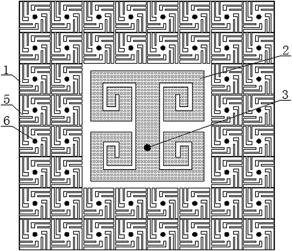
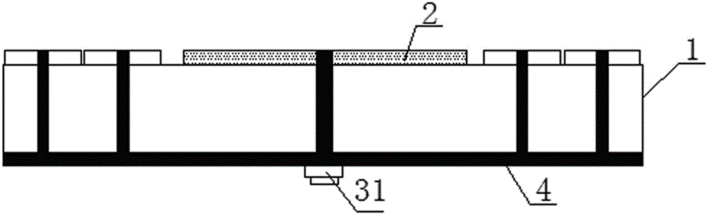
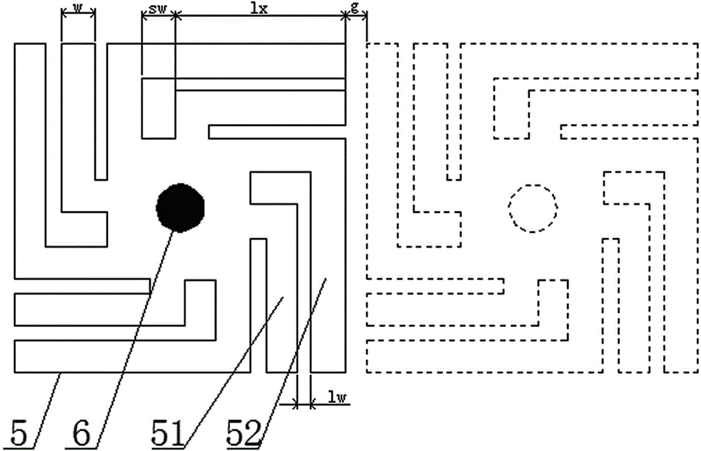
[0019] Such as Figure 1 to Figure 3 As shown, a microstrip patch antenna based on a photonic crystal structure includes a dielectric substrate 1, a metal ground layer 4 is provided on the back of the dielectric substrate 1, and a radiation branch 2 is provided in the center of the front of the dielectric substrate 1, and the radiation branch 2 is a mirror image Symmetrical four-helix structure, surrounded by a photonic crystal band gap layer, the photonic crystal band gap layer is set flush with the radiation branch 2, and the photonic crystal band gap layer consists of 2 rows (columns), a total of 48 metal patches arranged periodically 5, the metal patch 5 includes a central part, the center of the central part is connected to the metal ground layer 4 through a conductive via 6, and a plurality of L-shaped first metal microstrip lines 51 and The second metal microstrip line 52 and the metal ground layer 4 are connected to the radiation stub 2 through the feeding port 3 , and...


PUM


Abstract

The invention discloses a microstrip patch antenna based on a photonic crystal structure. The microstrip patch antenna comprises a dielectric substrate, wherein a metal grounding layer is arranged on the back side of the dielectric substrate; radiation branch nodes are arranged in the center of the front side of the dielectric substrate; the radiation branch nodes are of a four-helical structure in mirror symmetry; a photonic crystal forbidden band layer surrounds the radiation branch nodes; the photonic crystal forbidden band layer consists of a plurality of metal patches which are arranged in a periodic manner; the centers of the metal patches are connected with the metal grounding layer through conductive through holes; the metal grounding layer is connected with the radiation branch nodes through feed ports; signal transmission between the end parts of the feed ports and the outside can be achieved through SMA connectors. As the photonic crystal forbidden band layer is introduced around the radiation branch nodes, the defects that a microstrip patch antenna is low in gain and narrow in bandwidth are effectively solved, and moreover as the photonic crystal forbidden band layer is in certain distance from the radiation branch nodes, the mutual coupling is reduced, and the working property of the antenna is effectively ensured; in addition, due to the structure of the radiation branch nodes, current paths can be effectively increased, and the antenna can be minimized.

Description

technical field [0001] The invention belongs to the technical field of microstrip antennas, in particular to a microstrip patch antenna based on a photonic crystal structure. Background technique [0002] The concept of photonic crystals was proposed in the 1980s. Its biggest characteristic is that it has a forbidden band characteristic, that is, within the forbidden band range, it can suppress the surface waves propagating on its surface, or it does not support a certain frequency band. propagation of surface waves. Because of its small size, light weight, low profile, low cost, suitable for circuit integration and many other advantages, the microstrip antenna has been widely used in wireless communication systems, and plays its role in many fields such as mobile communication, satellite communication and aerospace. important role. But at the same time, some shortcomings of the microstrip antenna itself also limit its greater performance. Since the microstrip antenna is a...

Claims


Application Information

Patent Timeline
IPC IPC(8): H01Q1/38H01Q1/52
Inventor 滕兆朋刘志清张晓燕喻易强吴海龙殷星徐翠王学仁
Owner ZHONGTIAN BROADBAND TECH
Why Eureka
Try Eureka