Processing method of finished holes of circuit board with inner-layer copper thickness of more than 420 micrometers

A technology of inner layer copper thickness and processing method, which is applied in metal processing and other directions, can solve the problems that copper wire cannot be quickly dissipated and broken, CNC drilling machine is stuffy, and tool is broken, so as to solve the problem of inner layer pad falling off, drilling The effect of high hole feed rate and better chip breaking effect

Active Publication Date: 2015-06-10
DALIAN CHONGDA CIRCUIT
View PDF4 Cites 3 Cited by
  • Summary
  • Abstract
  • Description
  • Claims
  • Application Information

AI Technical Summary

Problems solved by technology

[0003] The salient feature of ultra-thick copper circuit boards is that the copper foil is very thick, especially for circuit boards with inner copper exceeding 420um, restricted by the special dry-cutting semi-closed drilling process of PCB, a large amount of copper foil will be generated during the drilling process. The cutting heat and the long copper wire cannot be dissipated and broken quickly, and it has been confirmed by slice analysis that this heat is enough to melt and carbonize the resin and glass cloth, so that the bonding force between the inner core material and the copper foil loss, resulting in the pad falling off and the product being discarded. At the same time, the cutting resistance of the ultra-thick copper springboard to the tool is also very large, especially for large-diameter drills above φ4.0mm, which often causes the spindle of the CNC drilling machine to "boring "turning" phenomenon, resulting in damage to the spindle and breaking of the tool, resulting in large losses

Method used


Image

  • Processing method of finished holes of circuit board with inner-layer copper thickness of more than 420 micrometers
  • Processing method of finished holes of circuit board with inner-layer copper thickness of more than 420 micrometers

Examples


Embodiment

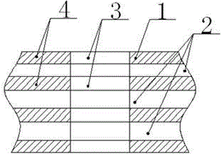
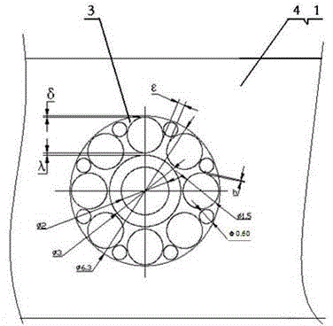
[0015] Embodiments, with reference to the accompanying drawings, a hole-forming method for a circuit board with an inner copper thickness of 420um or more, comprising a circuit board 4 with an inner copper thickness of 420um or more, bonded together by a multilayer copper foil layer 1 and a core material layer 2 , the method for processing the finished hole 3 on the circuit board 4 with an inner layer copper thickness of 420um or more is characterized in that the following steps are taken:

[0016] a. Choose a φ0.60mm drill bit, drilling speed 60-75krpm, feed 152-180ipm, return speed 1000ipm, drill multiple φ0.60mm holes evenly around the finished hole 3; cross-hole pause time 0ms; φ0. The distance between the 60mm hole and the finished hole 3 is δ, δ=30~50um;

[0017] b. After drilling φ0.60mm holes, select φ1.50mm drill bit, drilling speed 20~30krpm, feed 150~160ipm, return speed 1000ipm, drill multiple φ1.50mm holes between φ0.60mm holes, φ1. The distance between the 50m...


PUM


Abstract

The invention belongs to a processing method of finished holes of a circuit board with the inner-layer copper thickness of more than 420 micrometers. The processing method comprises the following steps: adopting a drilling head with phi 0.60 mm to uniformly drill a plurality of holes with phi of 0.60 mm around the finished holes (3) on the circuit board (4) of which the inner-layer copper thickness is more than 420 micrometers; adopting a drilling head with phi of 1.50 mm to drill a plurality of holes with phi of 1.50 mm; adopting a drilling head with phi of 2.00 mm to drill holes with phi of 2.00 mm at the centers of the finished holes (3); adopting a drilling head of 3.00 mm to drill holes with phi of 3.00 mm. The processing method disclosed by the invention has the advantages that the cutting force is effectively reduced, the drilling heat is lowered, and the problem that bonding pads on inner layers drop off is solved; the chip breaking effect is better; the phenomenon that copper wires wind cutters is avoided; the edges of the holes are smooth and tidy and do not have obvious burrs; the feeding rate of drilling is high.

Description

technical field [0001] The invention belongs to a method for forming a hole in a circuit board, in particular to a method for forming a hole in a circuit board with an inner layer copper thickness of more than 420um. Background technique [0002] With the rapid development of science and technology, thick copper plates above 100um and ultra-thick copper circuit boards above 420um have been more and more widely used and developed, because most of them are used in very important fields such as automobiles, electric power, and military industries. Therefore, the requirements for product quality reliability, stability, and heat resistance are extremely strict. However, because the processing of ultra-thick copper circuit boards is very difficult and the product rejection rate is very high, some circuit board companies have no ability to process them at all. [0003] The remarkable feature of ultra-thick copper circuit boards is that the copper foil is very thick, especially f...

Claims


Application Information

Patent Timeline
Patent Type & Authority Applications(China)
IPC IPC(8): B26F1/16
CPCB26F1/16
Inventor 纪龙江
Owner DALIAN CHONGDA CIRCUIT
Why Eureka
Try Eureka