Array substrate and liquid crystal display panel

An array substrate and matrix arrangement technology, which is applied in the field of liquid crystal displays, can solve problems such as uneven surface of the film layer, and achieve the effects of good flatness, elimination of adverse effects, and improvement of light leakage problems.

Inactive Publication Date: 2015-06-10
SHANGHAI TIANMA MICRO ELECTRONICS CO LTD +1
View PDF4 Cites 44 Cited by
  • Summary
  • Abstract
  • Description
  • Claims
  • Application Information

AI Technical Summary

Problems solved by technology

[0007] The technical problem to be solved by the present invention is to provide an array substrate and a liquid crystal display panel, which can solve the problem of uneven surface of the film layer above the touch wiring caused by the arrangement of the touch wiring, thereby eliminating the problem caused by the touch wiring. Adverse effects on the subsequent process caused by the setting of control wiring

Method used


Image

  • Array substrate and liquid crystal display panel
  • Array substrate and liquid crystal display panel
  • Array substrate and liquid crystal display panel

Examples


Embodiment 2

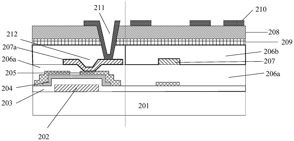
[0037] First introduce the array substrate corresponding to mid-com.

[0038] See figure 1 This figure is a cross-sectional view of an embodiment of the array substrate provided by the present invention.

[0039] The array substrate provided by this embodiment further includes: a first insulating layer 208, a pixel electrode layer 210, and a common electrode layer 209;

[0040] In addition, the array substrate further includes: a substrate 201, a gate 202, a gate insulating layer 203, and a semiconductor 204.

[0041] The common electrode layer 209 is located on the second flat layer 206b, the common electrode layer 209 includes a plurality of mutually independent touch electrodes, and each of the touch electrodes is connected to one or more touch electrodes. Line 207;

[0042] The first insulating layer 208 is located on the common electrode layer 209;

[0043] The pixel electrode layer 210 is located on the first insulating layer 208.

[0044] A metal pad 207a disposed on the first fla...

Embodiment 3

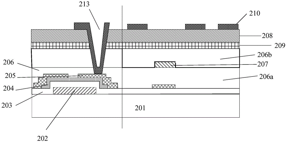
[0055] For details, see figure 2 As shown, this embodiment and figure 1 The difference in the illustrated embodiment is that figure 1 In the middle, the drain of the thin film transistor is indirectly electrically connected to the pixel electrode layer through two vias. In this embodiment, the drain of the thin film transistor is directly electrically connected to the pixel electrode layer through a via hole. When only one via hole is used for electrical connection, the penetration depth of the hole needs to be relatively deep, and the process is more complicated.

[0056] Such as figure 2 As shown, in this embodiment, a third via hole 213 penetrating through the first flat layer 206a and the second flat layer 206b is provided above the drain electrode 205 of the thin film transistor, and the pixel electrode layer 210 passes through the third via hole. The hole 213 is connected to the drain electrode 205 of the thin film transistor.

[0057] Array substrate embodiment four:

[005...


PUM

PropertyMeasurementUnit
thicknessaaaaaaaaaa

Abstract

The invention provides an array substrate and a liquid crystal display panel. The array substrate comprises a plurality of thin-film transistors, a first flat layer, a touch wire layer and a second flat layer, wherein the thin-film transistors are arrayed in a matrix manner; each thin-film transistor comprises a grid electrode, a source electrode and a drain electrode; the first flat layer covers the thin-film transistors; the touch wire layer is positioned on the first flat layer and comprises a plurality of touch wires; and the second flat layer is positioned on the touch wire layer. The problem that the surface of a film layer positioned above touch wires is not flat due to arrangement of the touch wires in the touch wire layer is solved, and harmful effects of arrangement of the touch wires on a follow-up manufacturing procedure are eliminated. The touch wires are positioned between the two flat layers, and an insulating layer which is adjacent to the touch wire layer is omitted. Only an insulating layer arranged between a common electrode and a pixel electrode remains. The second flat layer is arranged on the touch wires, so that the flatness of the portion above the touch wires is high, and friction light leakage is avoided. The touch wires can be thick, and the whole resistance of the touch wires is reduced.

Description

Technical field [0001] The present invention relates to the technical field of liquid crystal displays, in particular to an array substrate and a liquid crystal display panel. Background technique [0002] The main body of the current liquid crystal display panel includes a color filter substrate and an array substrate. In the production process of the array substrate, it is necessary to ensure the flatness of the surface pattern as much as possible to avoid inconvenience to the subsequent process. Therefore, a surface of the array substrate will be fabricated. Layer flat layer. [0003] However, for the liquid crystal display panel with integrated touch function, touch wiring needs to be added. The function of the touch trace is to connect each touch electrode to the touch drive chip. Wherein, the touch electrodes and the touch wires are generally not arranged on the same layer, and each touch wire passes through a via hole and is electrically connected to the touch electrode. ...

Claims


Application Information

Patent Timeline
Patent Type & Authority Applications(China)
IPC IPC(8): G02F1/1362G02F1/1368G02F1/1333G06F3/041
CPCG02F1/13338G02F1/136286G02F1/1368G06F3/0412G06F2203/04103G02F1/133345G06F3/0443G02F1/134372
Inventor 柴慧平袁永
Owner SHANGHAI TIANMA MICRO ELECTRONICS CO LTD
Why Eureka
Try Eureka