Manufacturing technology method for anti-latch-up groove type insulated gate bipolar transistor

A bipolar transistor and manufacturing process technology, applied in the field of electronics, can solve problems such as increasing device cost and reducing device competitive advantage, and achieve the effect of improving consistency, good consistency and reducing production cost

Inactive Publication Date: 2015-06-10
SHANGHAI HUAHONG GRACE SEMICON MFG CORP
View PDF4 Cites 3 Cited by
  • Summary
  • Abstract
  • Description
  • Claims
  • Application Information

AI Technical Summary

Problems solved by technology

[0003] At the same time, the traditional process requires more mask plates, which increases the cost of the device and reduces the competitive advantage of the device

Method used


Image

  • Manufacturing technology method for anti-latch-up groove type insulated gate bipolar transistor
  • Manufacturing technology method for anti-latch-up groove type insulated gate bipolar transistor
  • Manufacturing technology method for anti-latch-up groove type insulated gate bipolar transistor

Examples


Embodiment Construction

[0042] The present invention will be described in further detail below in conjunction with the accompanying drawings and embodiments.

[0043] A method for manufacturing a latch-resistant trench-type insulated gate bipolar transistor according to the present invention mainly includes the following steps:

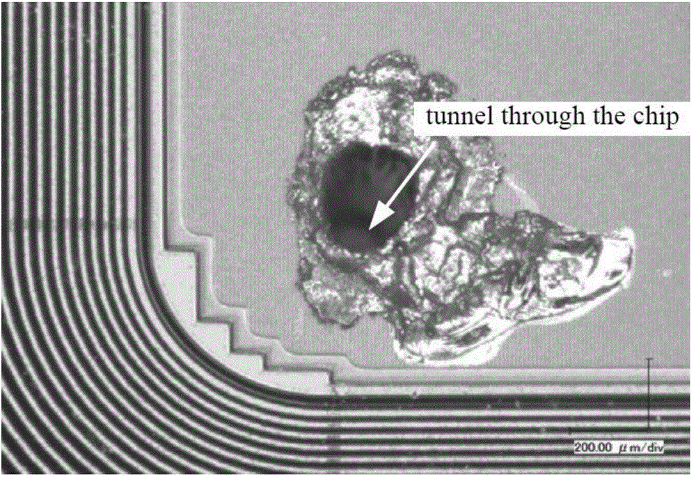
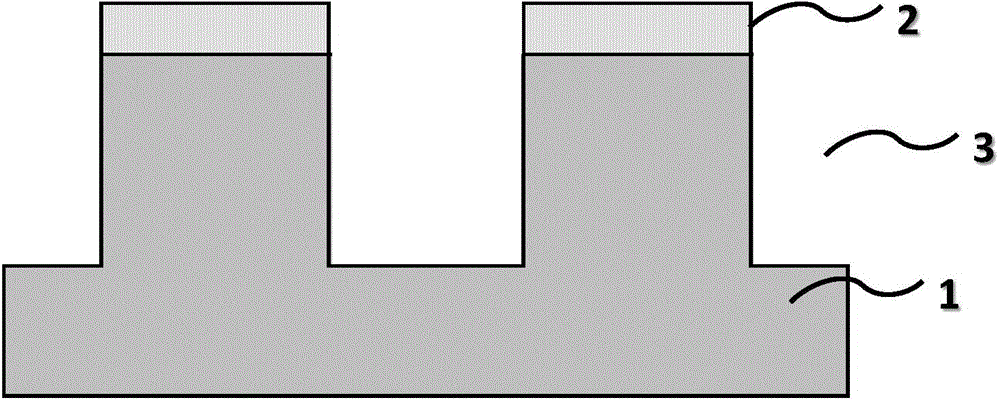
[0044] 1. If figure 1 As shown, a piece of silicon wafer is prepared as the silicon substrate 1. The parameters such as the type, thickness, resistivity, and pretreatment of the silicon wafer are all determined by the nature of the device design, that is, related to the device itself in the final application. The silicon wafer can be any Resistivity, the thickness of the silicon wafer is between 50 μm and 800 μm, and the silicon wafer is an epitaxial wafer, a Czochralski silicon wafer, a zone-melted silicon wafer, or an S.O.I silicon wafer. The pre-treatment includes terminal implantation, annealing, surface cleaning treatment and the like required by the design of the dev...


PUM


Abstract

The invention discloses a manufacturing technology method for an anti-latch-up groove type insulated gate bipolar transistor. A side wall technology is used for the groove type insulated gate bipolar field effect transistor, polycrystalline silicon which remains on the top of a groove and is exposed out of a silicon surface serves as a step, an oxide layer is deposited and is carved by a dry method to form a side wall, a base resistance adjusting region injection window is manufactured, base resistance between a channel and a source electrode is reduced, a reverse safe working region is optimized to a great degree, and consistency of the base resistance between different cellular structures is improved. Moreover, a special photomask for adjusting the base resistance is saved, and the technology is simplified.

Description

technical field [0001] The invention belongs to the field of electronic technology, and relates to power semiconductor devices, in particular to a manufacturing process method of a latch-resistant trench-type insulated gate bipolar transistor. Background technique [0002] The basic requirement of modern power devices is to be able to withstand high voltage and work with high current. Among them, the anti-latch-up ability of silicon-based power IGBT directly affects the overall performance of the device. However, the current traditional solution for optimizing the anti-latch-up ability of IGBTs uses an extra layer of injection mask, and after the injection is completed, a larger furnace tube is required to push the junction to adjust the base resistance. Because there is a certain alignment problem between the photomasks, the advancement of the furnace tube will also cause certain uneven problems, resulting in poor consistency in the anti-latch ability between different cel...

Claims


Application Information

Patent Timeline
Patent Type & Authority Applications(China)
IPC IPC(8): H01L21/336H01L21/265
CPCH01L29/66325H01L21/265H01L29/66333
Inventor 斯海国
Owner SHANGHAI HUAHONG GRACE SEMICON MFG CORP
Why Eureka
Try Eureka