Method for forming finned field effect transistor

A fin-type field effect and transistor technology, applied in semiconductor devices, semiconductor/solid-state device manufacturing, electrical components, etc., can solve the problems of uneven surface of the isolation layer and damaged fin contours, and achieve good surface flatness and flatness Excellent performance and improved performance

Active Publication Date: 2015-06-10
SEMICON MFG INT (SHANGHAI) CORP
View PDF3 Cites 0 Cited by
  • Summary
  • Abstract
  • Description
  • Claims
  • Application Information

AI Technical Summary

Problems solved by technology

[0013] The problem to be solved by the present invention is to provide a new method for forming a fin field effect transistor to solve the p

Method used


Image

  • Method for forming finned field effect transistor
  • Method for forming finned field effect transistor
  • Method for forming finned field effect transistor

Examples


Embodiment Construction

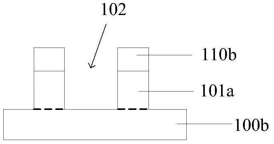
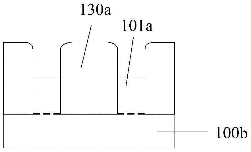
[0042] In the existing methods for forming fin field effect transistors, in the planarization process, the cap layer is usually removed first. At this time, if wet etching is used to etch the isolation material layer, the wet etching will also affect the fin portion. Etching, therefore, leads to poorer fin profile finally formed, and the poorer fin profile will affect the subsequently formed channel, ultimately affecting the performance of the transistor. If the isolation material layer is directly etched to form the isolation layer by using the SiConi etching method, since the isolation material layer has a part higher than the fin after the cap layer is removed (please refer to image 3 ), the SiConi etching method will simultaneously etch the upper surface and the exposed side of the isolation material layer (that is, the top corner of the isolation material layer is etched at 270 degrees), until the upper surface of the isolation material layer is lower than the fin. After...


PUM


Abstract

A method for forming a finned field effect transistor comprises the following steps of forming a cap layer on a semiconductor substrate; etching the cap layer and the semiconductor substrate until grooves are formed in the semiconductor substrate; forming fins on the semiconductor substrate and between the adjacent grooves; fully filling the grooves and covering the rest portion of the cap layer by using isolation material layers; flattening the isolation material layers until the isolation material layers are exposed out of the upper surface of the cap layer; etching the flattened isolation material layers for the first time until the upper surfaces of the rest isolation material layers are level and parallel to one another and are perpendicularly connected with a side surface of the cap layer; and etching the rest isolation material layers for the second time by using a SiConi etching method until isolation layers are formed. The fins of the finned field effect transistor formed by the method have good outlines, and the upper surfaces of the isolation layers are level and parallel to one another, so that the performance of the finned field effect transistor is improved.

Description

technical field [0001] The invention relates to the field of semiconductor technology, in particular to a method for forming a fin field effect transistor. Background technique [0002] With the continuous development of semiconductor industry technology, the adjustment of semiconductor device size has become the main factor to promote the improvement of integrated circuit manufacturing, and the structure of conventional MOS field effect transistors can no longer meet the requirements of device performance. The Fin Field Effect Transistor (FinFET) structure has attracted much attention due to its good cut-off performance, scalability, and compatibility with conventional fabrication processes. [0003] At present, fin field effect transistors can generally be divided into two categories: fin field effect transistors formed on semiconductor-on-insulator substrates (SOI), and fin field effect transistors formed on semiconductor substrates such as bulk silicon materials. Compar...

Claims


Application Information

Patent Timeline
IPC IPC(8): H01L21/336H01L21/28
CPCH01L29/06H01L29/66795
Inventor 童浩严琰
Owner SEMICON MFG INT (SHANGHAI) CORP
Why Eureka
Try Eureka