

Double-chip flip chip structure
A double-chip, flip-chip packaging technology, applied in the direction of electrical components, electrical solid-state devices, circuits, etc., can solve the problems of high cost, unfavorable heat dissipation, etc., and achieve the effects of saving energy, reducing chip packaging area, and reducing costs
- Summary
- Abstract
- Description
- Claims
- Application Information
AI Technical Summary
Problems solved by technology
Method used
Image

Examples
Embodiment
[0024] Embodiment: a double-chip flip-chip package package structure.
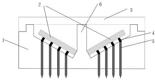
[0025] A double chip flip-chip packaging structure, refer to the attached figure 1 Shown: Including 1. Substrate 2. Chip 3. Heat sink 4. Conductive bump 5. Lead terminal 6. Central partition 7. Substrate top 8. Filler thermal conductive glue 9. Silver glue. It is characterized in that: the substrate 1 is made of insulating material and has a central partition 6, the chip 2 is placed in the slot formed by the central partition 6 and the top 7 of the substrate, and the lead terminal 5 passes through the depression of the 4 conductive bumps and the slope at the bottom of the slot. After melting, the electrical connection is made, and then the thermal conductive glue 8 is injected into the slot to cover the chip to protect the chip and transfer heat. The heat sink 3 is bonded to the central partition 6 and the top of the substrate 7 through silver glue 9 to form a double-chip flip-chip packaging structure.
PUM
 Abstract
Description
Claims
Application Information