Design method for converting PCI bus into ISA bus or APB bus

A technology of PCI bus and APB bus, which is applied in the field of bus interface conversion, can solve the problem that processors cannot access at the same time, and achieve the effect of optimal design, good adaptability and wide application range

Active Publication Date: 2015-06-17
FLIGHT AUTOMATIC CONTROL RES INST
View PDF4 Cites 8 Cited by
  • Summary
  • Abstract
  • Description
  • Claims
  • Application Information

AI Technical Summary

Problems solved by technology

[0005] The purpose of the present invention is to propose a design method for converting the PCI bus into an ISA and APB bus to solve the problem that the processor in the current embedded computer

Method used


Image

  • Design method for converting PCI bus into ISA bus or APB bus
  • Design method for converting PCI bus into ISA bus or APB bus
  • Design method for converting PCI bus into ISA bus or APB bus

Examples


Embodiment

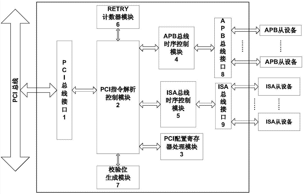
[0034] The IP core design method for converting PCI bus protocol to ISA and APB bus protocol is as follows: figure 1 As shown, the specific operation steps are as follows:

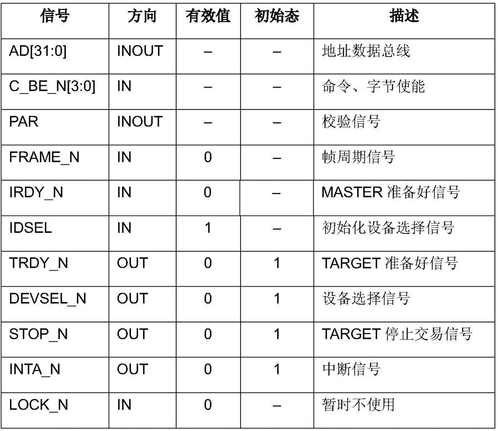
[0035] 1. PCI bus interface 1: realize the connection of PCI bus interface signals, see the specific signals figure 2 , and transmit the signal to the PCI instruction analysis control module 2 .

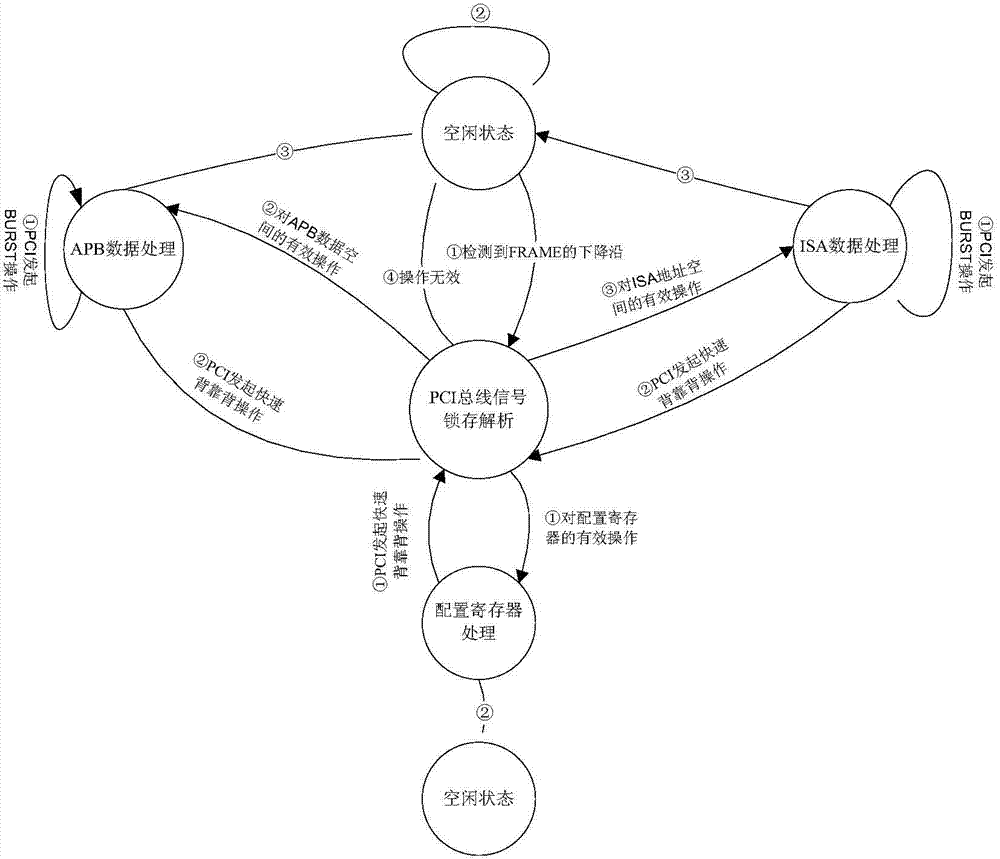
[0036] 2. PCI instruction analysis control module 2: see the state machine for its working process image 3 , first in the idle state, receive the PCI bus interface signals from PCI bus interface 1, and analyze these signals, when the falling edge of the FRAME signal is judged, enter the PCI bus signal latch analysis state, otherwise return to the idle state, and continue to wait . In the PCI bus signal latch analysis state, by analyzing the PCI bus command, determine which module is to be accessed in the following three modules. The three modules include: PCI configuration register processing module 3, APB b...


PUM


Abstract

The invention provides a design method for converting a PCI bus into an ISA bus or an APB bus. The design method solves the problem that in the prior art, a processor in an embedded type computer system cannot have access to devices meeting the ISA parallel bus protocol at the same time. According to the technical scheme, the design method comprises the steps that a PCI bus interface 1 receives a PCI bus configuration instruction of the PCI bus and sends the PCI bus configuration instruction to a PCI instruction analysis controlling module 2; the PCI instruction analysis controlling module 2 analyzes out a register address and a register memory address from the bus configuration instruction and sends the register address and the register memory address to a PCI bus configuration register module 3; the PCI bus configuration register module 3 writes the register address into a PCI control register which is located in the PCI bus configuration register module 3 and corresponds to the register address.

Description

technical field [0001] The present invention relates to the field of system-on-chip (System on Chip, "SoC") design, in particular to a bus interface conversion method. Background technique [0002] In a computer system, electronic chips and other components are interconnected by buses. Various components can be connected to a bus that enables communication between all devices connected to the bus. The various bus speeds in the computer are different, and the processor bus has a faster speed, which is used to connect faster peripherals such as processors and memories. The slower peripherals are attached to the processor bus bridge chip (also known as the North Bridge), which converts the high-speed processor bus into a lower-speed local bus. At present, the industry often uses the PCI bus as a local bus. [0003] However, these low-speed devices do not necessarily have PCI interfaces, and many device interfaces are ISA interfaces. This requires the design of an interface ...

Claims


Application Information

Patent Timeline
IPC IPC(8): G06F13/38G06F13/42
Inventor 陈浩左忠卫高尚
Owner FLIGHT AUTOMATIC CONTROL RES INST
Why Eureka
Try Eureka