Light emitting diode capable of achieving light mixing
A technology of light-emitting diodes and light mixing, which is applied in semiconductor devices, electrical components, circuits, etc., can solve the problems of uneven light mixing and insufficient light mixing, and achieve good uniformity
- Summary
- Abstract
- Description
- Claims
- Application Information
AI Technical Summary
Problems solved by technology
Method used
Image
Examples
Embodiment 1
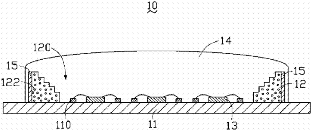
[0018] Such as figure 1 As shown, the substrate 11 is used to carry the light mixing device 12 and the LED die 13 . A circuit layer 110 is disposed on the substrate 11 . The substrate 11 can be a glass fiber board (FR4), a metal core printed circuit board (Metal Core PCB, MCPCB), a ceramic substrate (Ceramic Substrate), a silicon substrate (Silicon Substrate), a ceramic aluminum substrate (Ceramic Aluminum Substrate).
[0019] The light mixing device 12 is disposed around the LED die 13 . The light mixing device 12 is made of light-transmitting material, such as glass (Glass), polycarbonate (Polycarbonate, PC), polymethylmethacrylate (Polymethylmethacrylate, PSa), silicone resin (Silicone) or epoxy resin ( Epoxy Resin) and so on. The inside of the light mixing device 12 is doped with scattering particles 122, the refractive index of the scattering particles 122 is between 1.1 and 2.4, and its material can be titanium dioxide (TiO2), fused quartz (Fused Silica), polycarbonat...
Embodiment 2
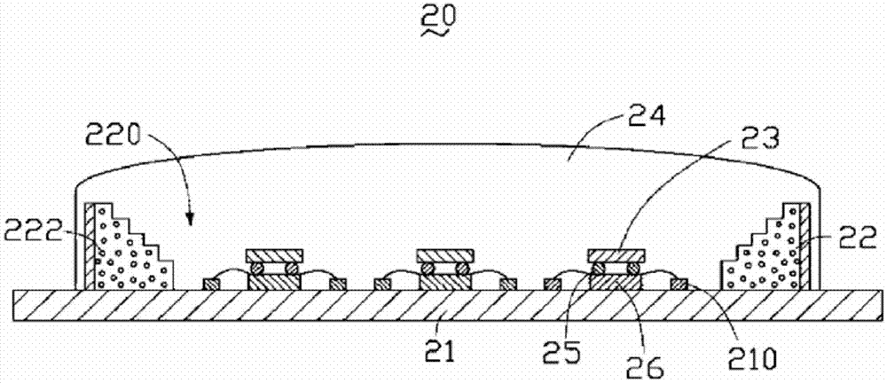
[0023] Such as figure 2 As shown, the second embodiment of the present invention also provides a light emitting diode 20, which includes a substrate 21, a light mixing device 22, a plurality of light emitting diode chips 23 and a package 24, the light emitting diode 20 and the above light emitting diode 10 are generally the same in structure, the difference is that the substrate 21 is provided with a plurality of substrate sub-substrates 26, and the plurality of light-emitting diode dies 23 are bonded to the substrate through metal bumps 25 by means of flip-chip (Flip Chip). The bottom sub-substrate 26 is electrically connected to the circuit layer 210 on the substrate 21 through metal wires (not shown).
[0024] It should be noted that the inner walls of the above-mentioned light mixing devices 12 and 22 facing the LED die 13 are not limited to be stepped surfaces, and may also be geometric surfaces of other shapes. see image 3 and Figure 4 , the embodiment of the prese...
PUM
 Abstract
Description
Claims
Application Information


