OLED device and encapsulating method thereof
A packaging method and device technology, which is applied in the manufacture of semiconductor devices, electrical solid devices, semiconductor/solid devices, etc., can solve the problems of high cost and difficult realization of glass frit packaging methods, and achieve the effect of reducing process difficulty and cost
- Summary
- Abstract
- Description
- Claims
- Application Information
AI Technical Summary
Problems solved by technology
Method used
Image
Examples
Embodiment 1
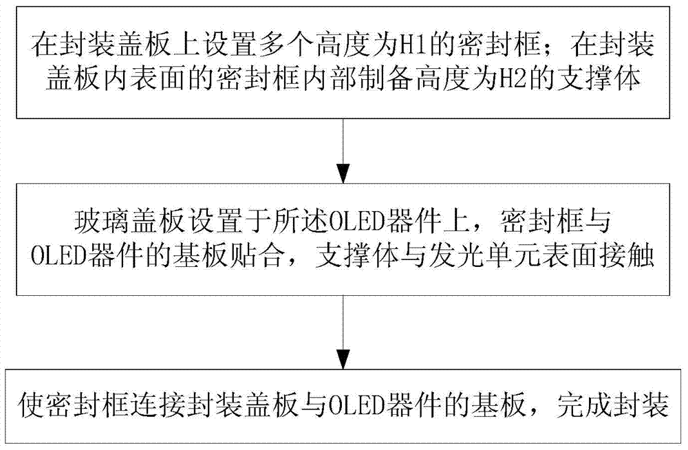
[0045] This embodiment provides a packaging method for an OLED device, such as image 3 shown, including the following steps:
[0046] S1: setting a plurality of sealing frames 403 with a height H1 on the packaging cover 400; preparing a support 401 with a height H2 inside the sealing frames 403 on the inner surface of the packaging cover 400.
[0047] S2: the packaging cover plate 400 is arranged on the OLED device, the sealing frame 403 is attached to the substrate 301 of the OLED device, and the support body 401 is in contact with the surface of the light emitting unit;
[0048] S3: Make the sealing frame 403 connect the packaging cover plate 400 and the substrate 301 of the OLED device, and complete the packaging. The above packaging method in this embodiment can ensure that when the packaging cover plate 400 is covered on the OLED device, the support body 401 and the The OLED device can be effectively contacted without generating too much pressure to cause damage to the...
Embodiment 2
[0061] On the basis of Example 1, in step S1 in this example, the glass frit used in the frit sealing frame includes V 2 o 5 ,P 2 o 5 , BaO, SiO 2 , B 2 o 3 、Al 2 o 3 , PbO, SnO, TeO 2 , MgO, CaO, ZnO, TiO 2 、WO 3 、 Bi 2 o 3 , Fe 2 o 3 , CuO, Sb 2 o 3 、Ru 2 O, Rb 2 O, any one or combination of lead borate glass, tin phosphate glass, vanadate glass and borosilicate. Wherein the size of the glass frit particles is greater than or equal to 0.1um and less than or equal to 10um. The above-mentioned glass frit can simultaneously meet various requirements such as packaging temperature, thermal expansion coefficient, thermal stability and chemical stability.
[0062] Further, in the step S12, the support body 401 is made of an organic polymer material, and the organic polymer is PI polyimide, epoxy resin, polyester, silicone resin, polycarbonate, aromatic Any one or a combination of heterocyclic polymers. The above-mentioned organic polymer materials all have cert...
Embodiment 3
[0064] On the basis of Embodiment 1 or Embodiment 2, the OLED device packaging method in this embodiment, the support body 401 in the step S12 is several pillars;
[0065] In the step S2, when the packaging cover plate 400 is placed on the OLED device, the contact point 701 between each pillar and the light emitting unit is located in the gap between two adjacent pixel subunits 305 place.
[0066]The pillars in this embodiment may be arranged in the same distribution manner as the pixel sub-units 305 , that is, there will be a contact point 701 in contact with the pillars between every two pixel sub-units 305 . It can also be set in such a way that there is a contact point 701 between every two pixel subunits 305 along the horizontal or vertical direction, such as Figure 7A and Figure 7C shown. This setting mode is simpler and more convenient for the preparation process. Or the setting method of the pillars adopts unequal intervals, such as Figure 7B and Figure 7D As...
PUM
 Abstract
Description
Claims
Application Information


