

Semiconductor device test structure and method of forming the same
A technology for device structure and test structure, which is applied in semiconductor devices, semiconductor/solid-state device manufacturing, semiconductor/solid-state device components, etc. Weak relay, etc.
- Summary
- Abstract
- Description
- Claims
- Application Information
AI Technical Summary
Problems solved by technology
Method used
Image

Examples
Embodiment Construction
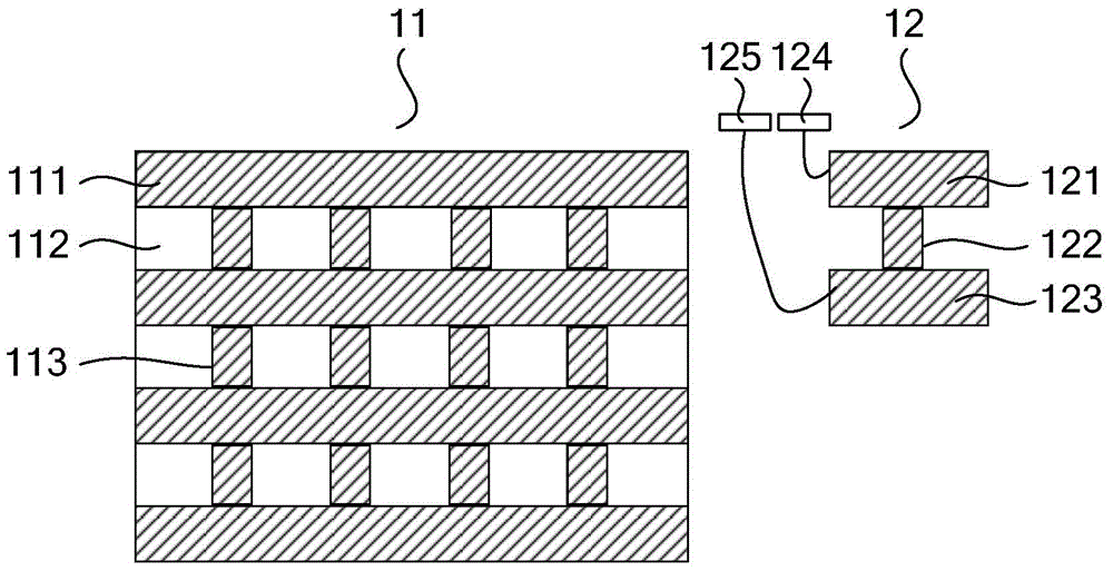
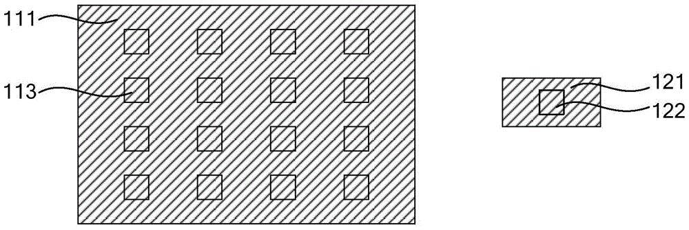
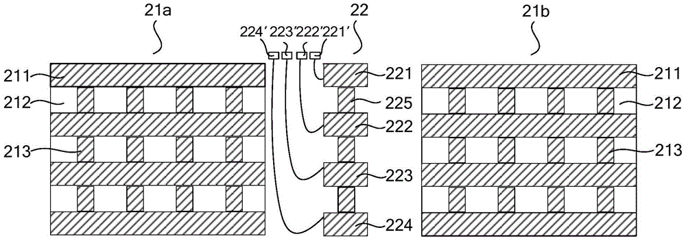
[0030] An embodiment of the present invention provides a test structure of a semiconductor device and a method for forming the same, the test structure includes a semiconductor device structure and a test unit, the semiconductor device structure includes multiple metal layers separated from each other in a dielectric layer, There is a first plug between two adjacent metal layers, the test unit is located in the dielectric layer on one side of the first semiconductor device structure, and the test unit is separated from the first semiconductor device structure The predetermined distance is used to obtain electrical characteristics corresponding to the dielectric layer between the multi-layer metal layers of the first semiconductor device structure.
[0031] In order to make the above objects, features and advantages of the present invention more comprehensible, specific embodiments of the present invention will be described in detail below in conjunction with the accompanying dr...
PUM
 Abstract
Description
Claims
Application Information