Storage card for surface-mounted component, feeder and automatic chip mounter
A surface mount and memory card technology, applied in the direction of electrical components, electrical components, etc., can solve the problems of small printed circuit boards and unsuitable packaging of small-sized chip components
- Summary
- Abstract
- Description
- Claims
- Application Information
AI Technical Summary
Problems solved by technology
Method used
Image
Examples
Embodiment 1
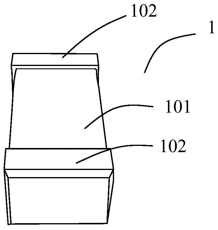
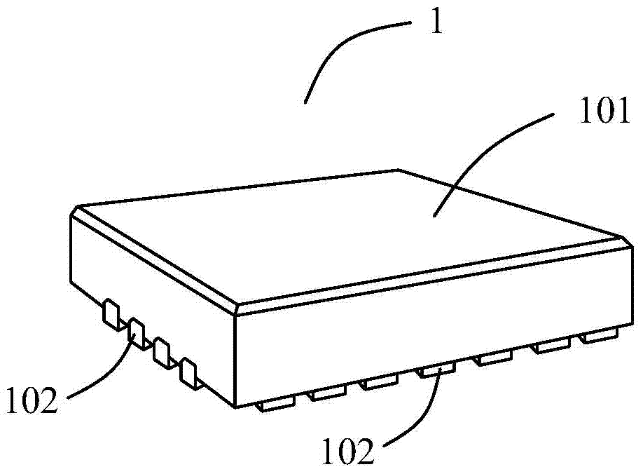
[0062] Such as Figure 7 to Figure 9 As shown, the card 60 is made of semi-rigid hard material like plastic sheet, paper sheet, etc., so as to keep the card 60 in the shape of a cuboid. The volume of the card 60 is 75*50*4mm, and it is used to place the chip component 1 of model 1206, and the volume of the chip component 1 is 3*1.5*1mm. The card 60 is provided with 37*21 component bins 57 vertically penetrating the front surface 51 and the rear surface 52 of the card 60, and a plurality of component bins 57 are regularly distributed with 21 per row and 37 per column, and each component The volume of the bin 57 is 1.7*1.1*4 mm, that is, the cross-section of the component bin 57 is slightly larger than the cross-section of the chip components 1 accommodated therein. A component bin 57 accommodates a chip component 1, and when the chip component 1 is loaded in the component bin 57 along its length direction, the chip component 1 and the component bin 57 are clearance fit, and th...
Embodiment 2
[0069] Such as Figure 10 to Figure 12 As shown, the card 70 is made of elastic materials such as rubber and sponge, and can also be made of semi-rigid materials such as foamed polyester to keep the card 70 in the shape of a cuboid. The volume of the card 70 is 100*50*4mm, and it is used to place the 0603 chip component 1, and the volume of the chip component 1 is 1.5*0.75*0.45mm. The card 70 is provided with 21*67 component bins 57 vertically penetrating the front surface 51 and the rear surface 52 of the card 70, and a plurality of component bins 57 are regularly distributed with 21 per row and 67 per column, and each component The volume of the bin 57 is 0.7*0.4*4mm, that is, the cross-section of the component bin 57 is slightly smaller than the cross-section of the chip components 1 accommodated therein. When the chip component 1 is loaded into the component bin 57 along its length direction under the action of external force, the chip component 1 and the component bin 57...
Embodiment 3
[0075] Such as Figure 14 As shown, the card 80 is made of hard materials such as plastic sheets and hard paper sheets, which can keep the card 80 in the shape of a cuboid, and can make the card 80 slightly deform under the action of external force, so that the chip component 1 It is fixed in the card 80 to prevent friction and collision between two adjacent chip elements 1; when the external force is removed, the card 80 can still return to its original shape; or, the card 80 is made of elastic material similar to rubber or sponge material, and a splint 510 made of hard material is pasted on the front surface 51 and the rear surface 52 of the card 80 to maintain the cuboid shape of the memory card. Due to the strong rigidity of the splint 510, when an external force is applied, the card 80 will Figure 16 or Figure 18 deform in that way to fix the chip component 1 in the card 80 . Conversely, cards can be made such as Figure 16 or Figure 18 In that shape, an external ...
PUM
| Property | Measurement | Unit |
|---|---|---|
| Volume | aaaaa | aaaaa |
Abstract
Description
Claims
Application Information


