Inter-chip high-speed interconnection link layer design method and system

A design method and link layer technology, applied in transmission systems, electrical components, etc., can solve problems such as slow interaction speed, poor performance, and low efficiency

Active Publication Date: 2015-07-08
FUZHOU ROCKCHIP SEMICON
View PDF3 Cites 6 Cited by
  • Summary
  • Abstract
  • Description
  • Claims
  • Application Information

AI Technical Summary

Problems solved by technology

[0005] To this end, it is necessary to provide a technical solution to realize the link layer of high-speed interconnection between chips to

Method used


Image

  • Inter-chip high-speed interconnection link layer design method and system
  • Inter-chip high-speed interconnection link layer design method and system
  • Inter-chip high-speed interconnection link layer design method and system

Examples


Embodiment Construction

[0048]In order to explain in detail the technical content, structural features, achieved goals and effects of the technical solution, the following will be described in detail in conjunction with specific embodiments and accompanying drawings.

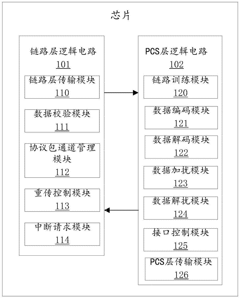
[0049] see figure 1 , is a schematic diagram of a chip of a link layer system implementing high-speed inter-chip interconnection according to an embodiment of the present invention. The chip includes a link layer logic circuit 101 and a PCS layer logic circuit 102; the link layer logic circuit 101 includes a data verification module 111, a protocol packet channel management module 112, and a link layer transmission module 110; the PCS layer The logic circuit 102 includes a link training module 120, a PCS layer transmission module 126, an interface control module 125, a data encoding module 121, a data decoding module 122, a data scrambling module 123 and a data descrambling module 124; the link layer logic circuit 101 is connected wit...


PUM


Abstract

The invention discloses an inter-chip high-speed interconnection link layer design method and system. The method is applied to an inter-chip high-speed interconnection link layer system. The system comprises a plurality of chips. The chips comprise link layer logic circuits and PCS layer logic circuits. The link layer logic circuits comprise data verification modules, protocol package channel management modules and link layer transmission modules. The PCS layer logic circuits comprise link training modules, PCS layer transmission modules, interface control modules, data coding modules, data decoding modules, data scrambling modules and data descrambling modules. The link layer logic circuits are connected with the PCS layer logic circuits. According to the design method and system, fast and efficient transmission of data among the multiple chips can be achieved.

Description

technical field [0001] The invention relates to the field of integrated circuit design, in particular to a link layer design method and system for realizing inter-chip high-speed interconnection. Background technique [0002] With the rapid development of semiconductor process technology, the performance of microprocessor (MCU), digital signal processor (DSP), programmable gate array (FPGA) has been greatly improved, making ultra-large-scale complex calculations in practice be more widely applied. But a single processor still cannot meet the growing application requirements. If multiple processors are interconnected into a processor array for multi-core cooperative parallel computing, the data processing capability of the system can be doubled, so the research on multi-core interconnection technology has become a new hot issue. [0003] Based on the link layer data transmission technology, although the technology has high complexity, it can realize the effective sharing of...

Claims


Application Information

Patent Timeline
IPC IPC(8): H04L29/08H04L29/06
Inventor 李仙辉张明懿
Owner FUZHOU ROCKCHIP SEMICON
Why Eureka
Try Eureka