Array substrate, manufacturing method thereof, and display device

A technology of an array substrate and a manufacturing method, which is applied in the display field and can solve the problems of difficult data line pattern precise etching, too wide data line pattern 4a, and inability to realize display control, etc.

Active Publication Date: 2018-07-20
BOE TECH GRP CO LTD +1
View PDF5 Cites 0 Cited by
  • Summary
  • Abstract
  • Description
  • Claims
  • Application Information

AI Technical Summary

Problems solved by technology

However, the existing etching process is difficult to ensure accurate etching of the data line pattern, which may cause the etched data line pattern 4a to be too wide and connected to the pixel electrode pattern 5a (see figure 2 ), unable to achieve display control

Method used


Image

  • Array substrate, manufacturing method thereof, and display device
  • Array substrate, manufacturing method thereof, and display device
  • Array substrate, manufacturing method thereof, and display device

Examples


Embodiment Construction

[0040] In order to make the purpose, technical solutions and advantages of the embodiments of the present invention clearer, the technical solutions in the embodiments of the present invention will be clearly and completely described below in conjunction with the drawings in the embodiments of the present invention. Obviously, the described embodiments It is only some embodiments of the present invention, but not all embodiments. Based on the embodiments of the present invention, all other embodiments obtained by persons of ordinary skill in the art without creative efforts fall within the protection scope of the present invention.

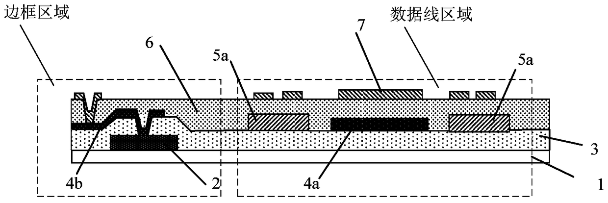
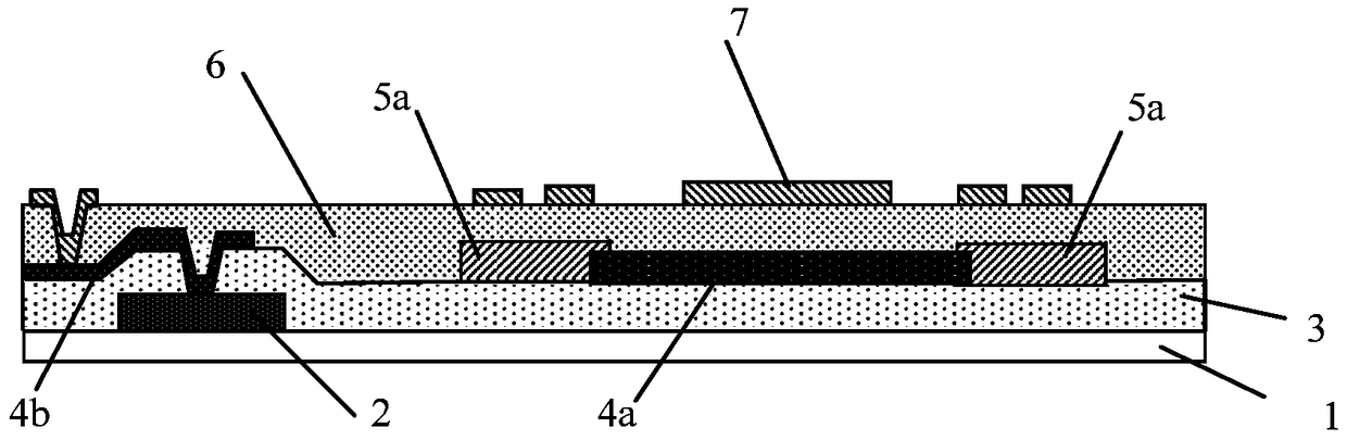
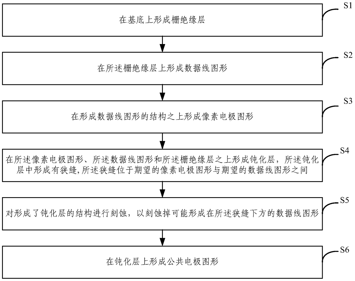
[0041] An embodiment of the present invention provides a method for fabricating an array substrate, which can be used to fabricate an ADS array substrate, such as image 3 As shown, the method includes:

[0042] Step S1, forming a gate insulating layer on the substrate;

[0043] Step S2, forming a data line pattern on the gate insulating layer; ...


PUM


Abstract

The invention provides an array substrate and a manufacturing method thereof as well as a display device. The manufacturing method comprises the following steps: forming a grilling insulation layer; forming a data cable figure on the grilling insulation layer; forming a pixel electrode figure on the structure of the formed data cable figure; forming a passivation layer on the data cable figure and the grilling insulation layer; forming a slot in the passivation layer, wherein the slot is formed between the supposed pixel electrode figure and the supposed data cable figure; etching the structure of the formed passivation layer to eliminate the data cable figure formed under the slot; forming a common electrode figure on the passivation layer. According to the manufacturing method, the data cable figure can be prevented from being connected with the pixel electrode figure.

Description

technical field [0001] The present invention relates to the field of display technology, in particular to an array substrate, a manufacturing method thereof, and a display device. Background technique [0002] Advanced Super Dimension Switch (ADSDS, ADS for short) technology is to form a multi-dimensional electric field through the electric field generated by the edge of the slit electrode in the same plane and the electric field generated between the slit electrode layer and the plate electrode layer. All oriented liquid crystal molecules between the slit electrodes in the liquid crystal cell and directly above the electrodes can be rotated, thereby improving the working efficiency of the liquid crystal and increasing the light transmission efficiency. Advanced ultra-dimensional field conversion technology can improve the thin film field effect transistor liquid crystal display ( Thin Film Transistor-Liquid Crystal Display, TFT-LCD) product picture quality, with high resolu...

Claims


Application Information

Patent Timeline
Patent Type & Authority Patents(China)
IPC IPC(8): H01L21/77H01L27/12
CPCH01L27/1214H01L27/124H01L27/1259
Inventor 孙志宋瑞涛
Owner BOE TECH GRP CO LTD
Why Eureka
Try Eureka