

Etching solution for photoelectrochemical etching of gallium nitride
A technology of photoelectrochemistry and etching solution, applied in the direction of chemical instruments and methods, circuits, electrical components, etc., can solve the problems of large material damage, cost and energy loss, and environmental adverse effects
- Summary
- Abstract
- Description
- Claims
- Application Information
AI Technical Summary
Problems solved by technology
Method used
Image

Examples
Embodiment 1
[0041] This embodiment provides an etching solution for photoelectrochemical etching of gallium nitride, wherein glycine is used as an etchant, deionized water is used as a solvent, and glycine is dissolved in deionized water to form an etching solution.
[0042] Specifically, in this embodiment, the weight percentage of glycine is 20%, the weight percentage of deionized water is 80%, and a saturated glycine aqueous solution is prepared as an etching solution. The etching solution of this embodiment does not add additives.
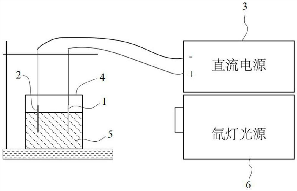
[0043] In this embodiment, the above-mentioned etching solution is used to perform photoelectrochemical etching on the gallium nitride epitaxial wafer, including the following steps:
[0044] (1) Soak a 1.1cm×0.3cm GaN epitaxial wafer in aqua regia and wash it for 5 minutes.
[0045] (2) Put the GaN epitaxial wafer obtained in step (1) into acetone, ethanol, and deionized water in sequence for ultrasonic cleaning for 15 minutes each.
[0046] (3) Using a...
Embodiment 2
[0055] This embodiment provides an etchant for photoelectrochemical etching of gallium nitride, wherein L-glutamic acid is used as an etchant, formic acid is used as a solvent, and L-glutamic acid is dissolved in formic acid to form an etching solution. liquid.
[0056] Specifically, in this embodiment, the weight percentage of L-glutamic acid is 20%, the weight percentage of formic acid is 80%, and a saturated L-glutamic acid formic acid solution is prepared as an etching solution. The etching solution of this embodiment does not add additives.
[0057] In this embodiment, referring to the etching process steps (1) to (6) in Embodiment 1, the GaN epitaxial wafer is photoelectrochemically etched using the etching solution as described above in this embodiment.
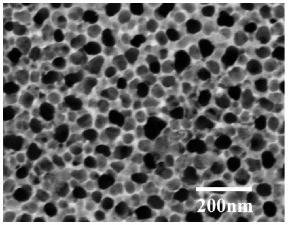
[0058] Figure 4 It is the SEM picture of the GaN epitaxial wafer after etching in this embodiment, as Figure 4 shown, with figure 2 Compared with this GaN epitaxial wafer, the hierarchical structure of the etche...
Embodiment 3
[0060] This embodiment provides an etching solution for photoelectrochemical etching of gallium nitride, wherein methyl aspartame is used as an etchant and citric acid is used as a solvent to dissolve methyl aspartame Form etchant in citric acid. The etching solution of this embodiment also added 1-ethyl-3-methylimidazolium trifluoromethanesulfonate as an auxiliary agent.
[0061] Specifically, the percentage by weight of aspartame in the present embodiment is 15%, the percentage by weight of formic acid is 80%, and the percentage by weight of 1-ethyl-3-methylimidazole trifluoromethanesulfonate is 5%. %, prepared as saturated aspartame citric acid solution as etching solution.
[0062] In this embodiment, referring to the etching process steps (1) to (6) in Embodiment 1, the GaN epitaxial wafer is photoelectrochemically etched using the etching solution as described above in this embodiment.
PUM
| Property | Measurement | Unit |
|---|---|---|
| Aperture | aaaaa | aaaaa |
| Average pore size | aaaaa | aaaaa |
| Average pore size | aaaaa | aaaaa |
Abstract
Description
Claims
Application Information