Filler and Surface Treatment Method of Chip Components

A surface treatment and filler technology, applied in electrical components, electrical solid devices, semiconductor devices, etc., can solve the problems of increasing the nickel layer of the intermediate layer, difficulty, reducing the probability of tin spraying phenomenon, etc., to achieve strong hydrophobic performance, use Simple, anti-corrosion effect

Active Publication Date: 2018-02-16
SHENZHEN ZHENHUA FU ELECTRONICS
View PDF3 Cites 0 Cited by
  • Summary
  • Abstract
  • Description
  • Claims
  • Application Information

AI Technical Summary

Problems solved by technology

The electroplating solution remaining in the micropores of the terminal has a great adverse effect on the reliability of the product
[0003] For the above problems, there are two traditional treatment methods: one is to improve the material and proportion of the slurry layer, reduce the porosity of the slurry layer after sintering, improve the compactness, and achieve the purpose of reducing the solution entering the electrode pores. However, due to the sintering of the slurry, there will be gas escape, and the pores on the surface and inside of the electrode are inevitable, so that the effect of this kind of improvement is very limited and it is extremely difficult; the other is to increase the thickness of the nickel layer in the middle layer. The method can only reduce the probability of tin spraying when the product is mounted, but cannot prevent the solution entering the electrode from corroding the connecting electrode and causing electrical performance failure, and increasing the thickness of the nickel layer will lead to an increase in cost

Method used


Image

  • Filler and Surface Treatment Method of Chip Components
  • Filler and Surface Treatment Method of Chip Components
  • Filler and Surface Treatment Method of Chip Components

Examples


preparation example Construction

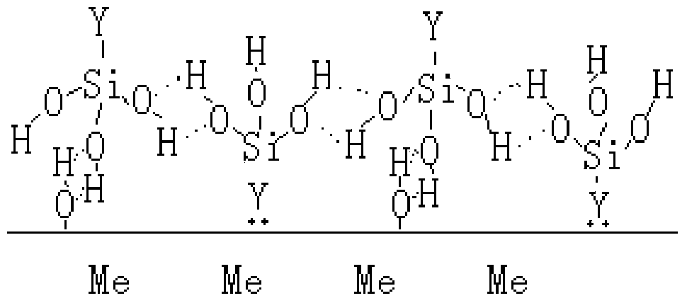
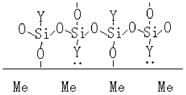
[0048] The preparation method of above-mentioned filler comprises the steps:

[0049] 60-75 parts by weight of alcohol and 5-10 parts by weight of water are prepared into an aqueous alcohol solution;

[0050] Mixing 15-30 parts by weight of vinyl silane coupling agent and alcohol aqueous solution to obtain a mixed solution;

[0051] Add 1-5 parts by weight of organic carboxylic acid to the mixed liquid.

[0052] The preparation method of the above filler is relatively simple.

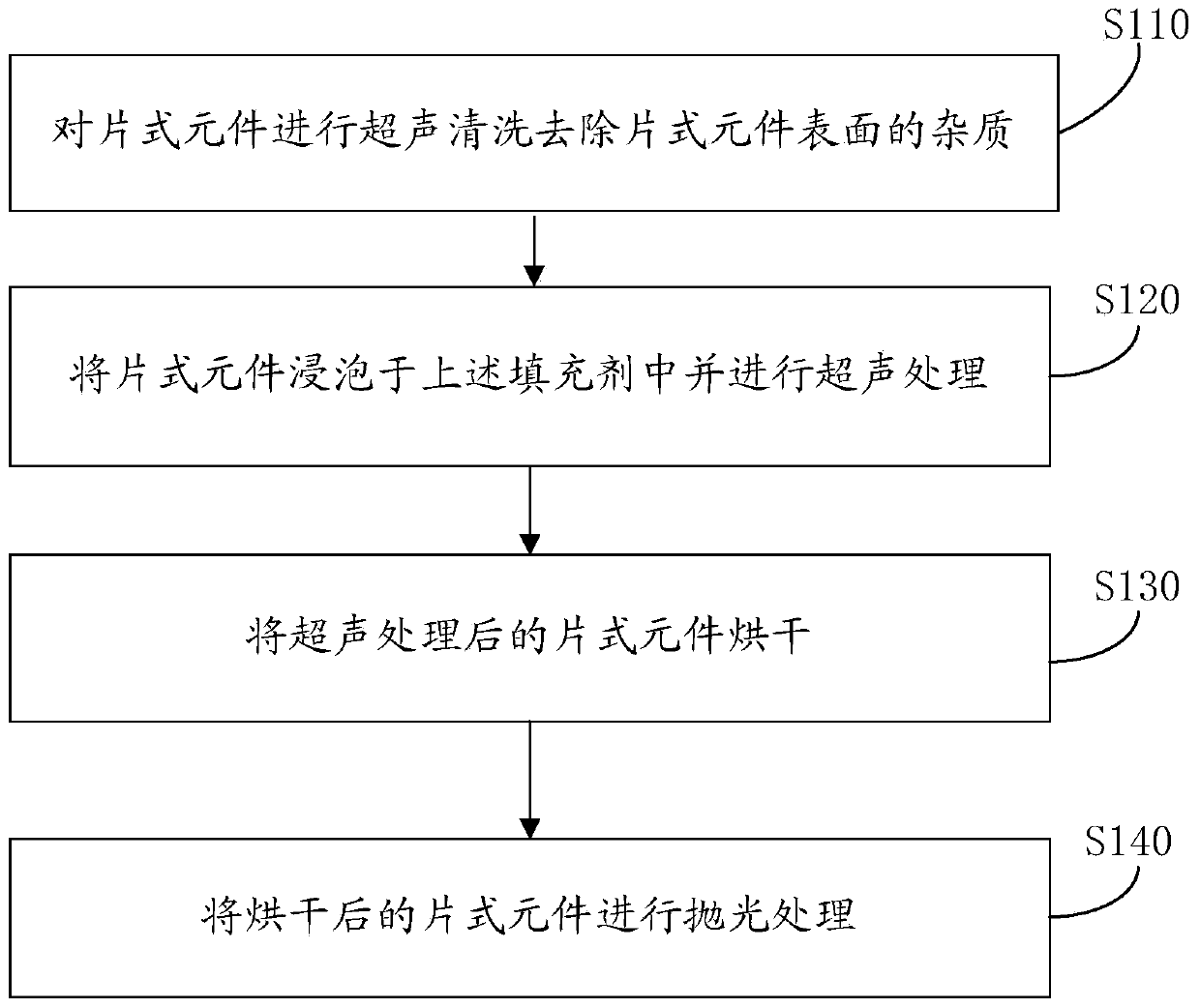
[0053] The surface treatment method of the chip component using the above-mentioned filler in one embodiment includes the following steps:

[0054] Step S110, performing ultrasonic cleaning on the chip component to remove impurities on the surface of the chip component.

[0055] The chip components involved in this embodiment are chip components in laminated inductors, capacitors, and resistors. The terminal electrodes generally adopt three-layer electrode technology, which is composed of three-layer e...

Embodiment 1

[0072] 1. Take the end-capped and sintered multilayer chip inductor (silver end), ultrasonically clean it in deionized water for 7 minutes, remove surface impurities, and then dry it.

[0073] 2. Soak the cleaned and dried chip inductor at room temperature in the filler for ultrasonic treatment for 8 minutes.

[0074] The composition of the filler is: in parts by mass, 20 parts of vinyltriethoxysilane, 70 parts of ethanol, 8 parts of water, 2 parts of acetic acid, and the pH value is 5.0.

[0075] 3. Dry the soaked chip inductor at 110°C for 70 minutes.

[0076] 4. Polish the dried chip inductor for 30 minutes.

Embodiment 2

[0078] 1. Take the capped and sintered chip inductor (silver terminal), ultrasonically clean it in deionized water for 6 minutes, remove surface impurities, and then dry it.

[0079] 2. Soak the cleaned and dried chip inductor at room temperature in the above-mentioned filler for ultrasonic treatment for 10 minutes.

[0080] The composition of the filler is: in parts by mass, 15 parts of vinyltriethoxysilane, 75 parts of ethanol, 5 parts of water, 5 parts of acetic acid, and the pH value is 4.0.

[0081] 3. Dry the soaked chip inductor at 120°C for 60 minutes.

[0082] 4. Polish the dried chip inductor for 25 minutes.


PUM


Abstract

The invention provides a filling agent and a surface treatment method of chip components. A filler comprises the following components in parts by mass: 15-30 parts of vinyl silane coupling agent; 60-75 parts of alcohol; 5-10 parts of water; 1-5 parts of organic carboxylic acid. The above-mentioned filler can seal the micropores on the surface of the chip component.

Description

technical field [0001] The invention relates to a filler and a method for surface treatment of a chip component using the filler. Background technique [0002] With the rapid development of modern science and technology and the information industry, electronic components are used more and more widely, and the amount used is increasing. At the same time, the rapid development of automotive electronics, communication navigation, aerospace and other industries has put forward higher and higher requirements for the reliability of electronic components. The quality of the terminal electrodes of electronic components has an important impact on reliability indicators such as electrical properties and welding performance. As the three basic electronic components, chip inductors, capacitors, and resistors generally use three-layer terminal electrode technology in the manufacturing process. The three-layer terminal electrode consists of three layers of electrodes: a base electrode (...

Claims


Application Information

Patent Timeline
Patent Type & Authority Patents(China)
IPC IPC(8): H01L23/16H01L21/54
Inventor 欧爱良樊应县朱建华高永毅尹红葵曹华春王智会
Owner SHENZHEN ZHENHUA FU ELECTRONICS
Why Eureka
Try Eureka