
A Realization Method of Space Vector Modulation Based on Combination of Digital and Analog

A technology of space vector modulation and implementation method, which is applied in the field of power electronics and electric transmission, and can solve problems such as longer upgrade cycle, higher cost, and inability to directly apply research results.

Active Publication Date: 2017-10-03
中国东方电气集团有限公司
View PDF2 Cites 0 Cited by
  • Summary
  • Abstract
  • Description
  • Claims
  • Application Information

AI Technical Summary

Problems solved by technology

Because many of the existing control platforms do not have dedicated PWM generation hardware resources, the current research results cannot be directly applied, so it is necessary to redevelop the control platform with high-performance controllers, or add new circuit boards to realize SVPWM, which will inevitably lead to Increased costs, longer upgrade cycles, etc.

Method used


Image

  • A Realization Method of Space Vector Modulation Based on Combination of Digital and Analog
  • A Realization Method of Space Vector Modulation Based on Combination of Digital and Analog
  • A Realization Method of Space Vector Modulation Based on Combination of Digital and Analog

Examples


Embodiment 1

[0072] A digital-analog combined space vector modulation implementation method uses an ordinary digital controller to complete the sector judgment, vector action time calculation and switch time calculation in the SVPWM algorithm, and completes the output setting according to the carrier characteristics of the subsequent hardware circuit. Level analog circuit realizes the generation of PWM pulse.

[0073] The specific steps are:

[0074] The first step is to judge the instruction space vector U OUT Sector N;

[0075] The second step is to calculate the conventional vector action time t X , t Y and zero vector action time t 0 ;

[0076] t 0 is not a regular vector, but a zero vector.

[0077] The third step is to calculate the switching point or switching time waveform t of each phase pulse cm1 , t cm2 , t cm3 ;

[0078] The fourth step is to combine the switching time waveform obtained in the third step with the carrier characteristics of the subsequent hardware cir...

Embodiment 2

[0081] A digital-analog combined space vector modulation implementation method, using a conventional controller to complete the sector judgment, vector action time calculation and switch time calculation in the SVPWM algorithm, and complete the output setting according to the carrier characteristics of the subsequent hardware circuit, and finally pass the Level hardware circuit realizes the generation of PWM pulse.

[0082] The specific steps are:

[0083] 1) Judging the command voltage space vector U OUT The sector number N.

[0084] The command voltage space vector U OUT In response to load disturbances and command changes, the power electronic converter is the command control quantity obtained by closed-loop adjustment according to the real-time parameters of the system.

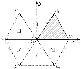
[0085] The sector number N refers to the position area of ​​any voltage space vector on the space plane. According to the angle θ between the voltage space vector and the α axis of the stationary coord...


PUM


Abstract

The invention relates to the technical field of electric transmission and control, in particular to a digital-analog combined SVPWM (space vector pulse width modulation) method. The method includes the steps of a, judging a sector of an instruction space vector; b, calculating acting time of a conventional space vector; c, calculating on-off time of each phase of pulse; d, according to hardware carrier features, subjecting waveform of the on-off time calculated in the former step to output setting, allowing outputting to a hardware board, and generating PWM through carrier comparison. The method has the advantages that implementation base on a common digital controller and a common hardware carrier modulation board needs no high-performance digital processor having PWM generation related hardware resources, thus cost is reduced; algorithm upgrading is facilitated for part of existing power electronic converter control systems, upgrading cost is reduced, and upgrading period is shortened.

Description

technical field [0001] The invention relates to the field of power electronics and electric transmission, and specifically relates to a method for realizing a digital-analog combined space vector modulation (SVPWM). Background technique [0002] In the field of power electronics and power transmission, pulse width modulation (PWM) is often used to obtain the required command voltage. After decades of development, people have developed a variety of PWM modulation techniques, and the development of power electronic devices and the application of microprocessors in the control of power electronic converters provide a broad research and open space for PWM technology. Different PWM modulation techniques correspond to different performance indicators, among which the three key indicators are: output voltage harmonic distribution, switching loss of switching devices, and DC link voltage utilization. [0003] Space vector pulse width modulation (space vector pulse width modulation,...

Claims


Application Information

Patent Timeline
Patent Type & Authority Patents(China)
IPC IPC(8): H02M7/5395H02P21/00H02P27/12
CPCH02M7/5395
Inventor 代同振周宏林吴小田于海坤
Owner 中国东方电气集团有限公司
Learn More