Flexible transfer method of photonic crystal or micro/nano grating structure on end surface of optical fiber
A technology of photonic crystal and grating structure, applied in cladding optical fiber, optical waveguide, light guide, light guide, etc., can solve the problem of small size of the end face of the optical fiber, achieve probe-based, precise control and skills, miniaturization and integration Effect
- Summary
- Abstract
- Description
- Claims
- Application Information
AI Technical Summary
Problems solved by technology
Method used
Image

Examples
example 1
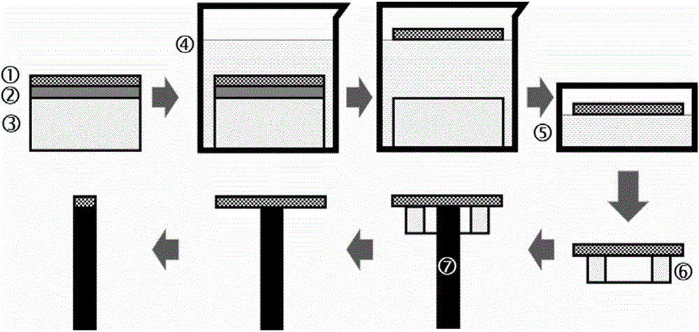
[0043] Example 1: Stripping transfer of photonic crystals on fiber end faces.
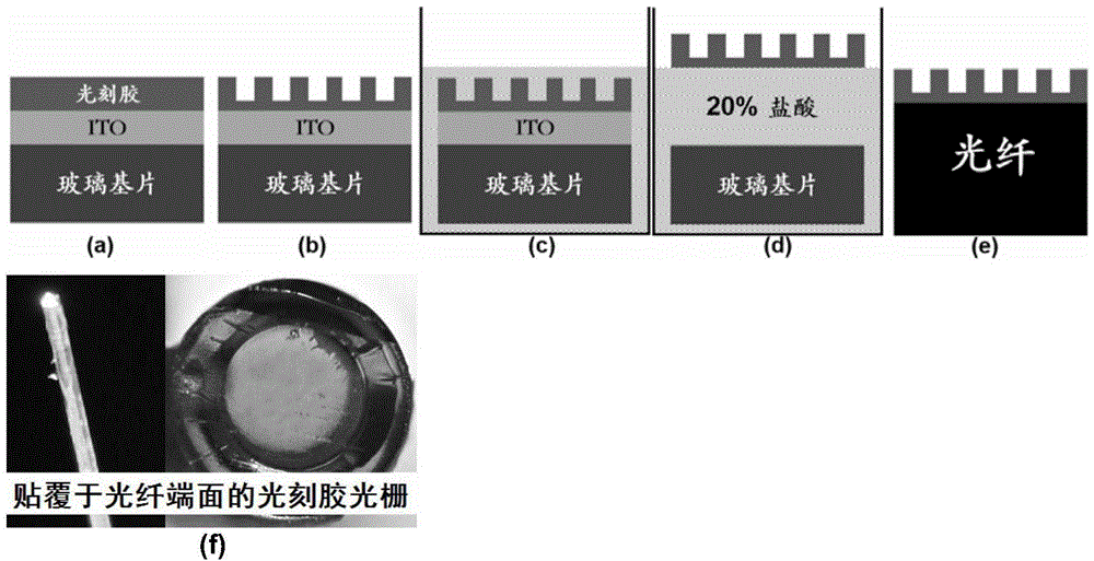
[0044] (1) Use interference lithography to create a surface with an area of 10×10mm 2 A photoresist grating structure with a period of 500 nm was prepared on the surface of the ITO glass. The interference lithography uses a He-Cd laser with an output wavelength of 325nm as the ultraviolet light source, and S1805 photoresist as the recording medium. S1805 is spin-coated on the surface of ITO glass at a speed of 2000 revolutions per second, and its thickness is about 500nm. See image 3 (a).
[0045] (2) Control the exposure and development time so that the modulation depth of the photoresist grating is about 300nm. See image 3 (b).
[0046] (3) Soak the photoresist grating sample in 20% hydrochloric acid for 60 minutes. See image 3 (c).
[0047](4) The ITO film is completely dissolved, and the photoresist grating is separated from the substrate and floats on the surface of the hydrochlo...
example 2
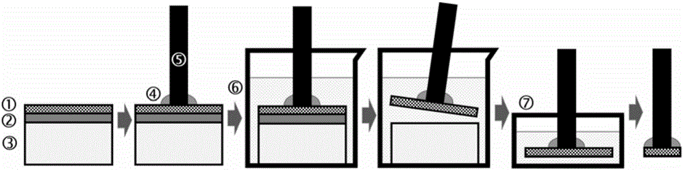
[0051] Example 2: Welding transfer of metal photonic crystals on the end face of optical fiber.
[0052] (1) obtain photoresist grating ( Figure 4 (a) Colloidal solution of chemically synthesized gold nanoparticles in toluene was spin-coated at a concentration of 100 mg / ml. See Figure 4 (b).
[0053] (2) The sample was heated in a muffle furnace at 300° C. for 20 minutes, and then naturally cooled to room temperature to obtain a metal photonic crystal with a period of 500 nm. See Figure 4 (c).
[0054] (3) An optical fiber with a core diameter of 400 μm is fixed above the metal photonic crystal, so that the end face of the optical fiber is in natural contact with the upper surface of the metal photonic crystal. See Figure 4 (d).
[0055] (4) Drop a small amount of PMMA chloroform solution at the contact point between the optical fiber and the metal photonic crystal, with a concentration of 15 mg / ml. Stand still in the fume hood for 100 minutes to fully evaporate th...
PUM
| Property | Measurement | Unit |
|---|---|---|
| Thickness | aaaaa | aaaaa |
| Thickness | aaaaa | aaaaa |
| Concentration | aaaaa | aaaaa |
Abstract
Description
Claims
Application Information
 - R&D Engineer
- R&D Manager
- IP Professional
- Industry Leading Data Capabilities
- Powerful AI technology
- Patent DNA Extraction
Browse by: Latest US Patents, China's latest patents, Technical Efficacy Thesaurus, Application Domain, Technology Topic.
© 2024 PatSnap. All rights reserved.Legal|Privacy policy|Modern Slavery Act Transparency Statement|Sitemap