Chip fuse and manufacturing method of chip fuse

A manufacturing method and technology of fuses, applied in fuse manufacturing, emergency protection device manufacturing, electrical components, etc., can solve problems such as hard protective film and impact damage

Active Publication Date: 2017-10-24
KAMAYA ELECTRIC
View PDF3 Cites 0 Cited by
  • Summary
  • Abstract
  • Description
  • Claims
  • Application Information

AI Technical Summary

Problems solved by technology

Since the protective films 7, 8, and 9 formed of epoxy resin are relatively hard, they are easily damaged by the above-mentioned impact.

Method used


Image

  • Chip fuse and manufacturing method of chip fuse
  • Chip fuse and manufacturing method of chip fuse
  • Chip fuse and manufacturing method of chip fuse

Examples


Embodiment Construction

[0090] Hereinafter, embodiments of the present invention will be described in detail based on the drawings.

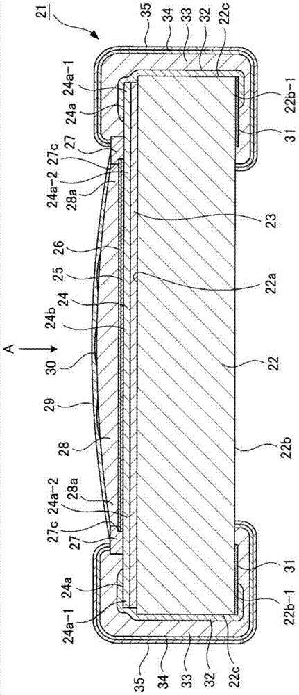
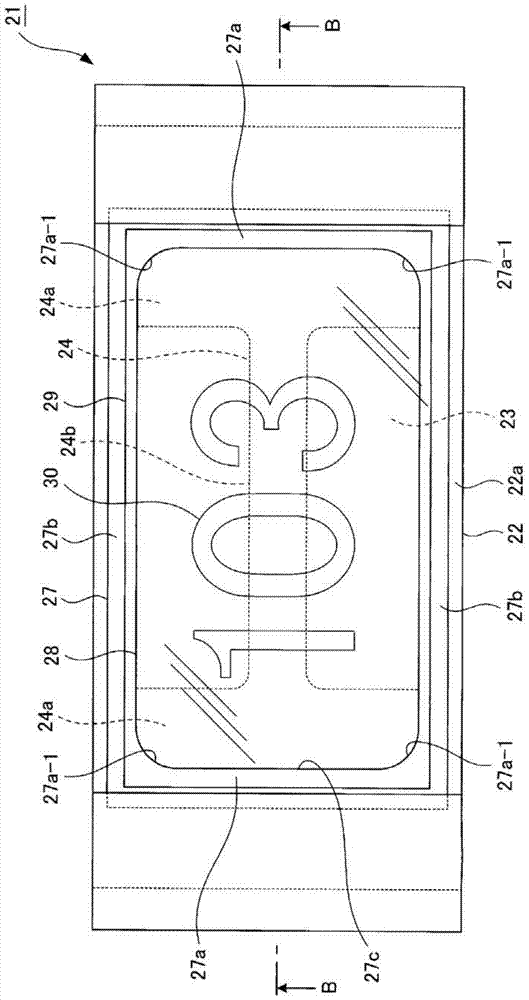
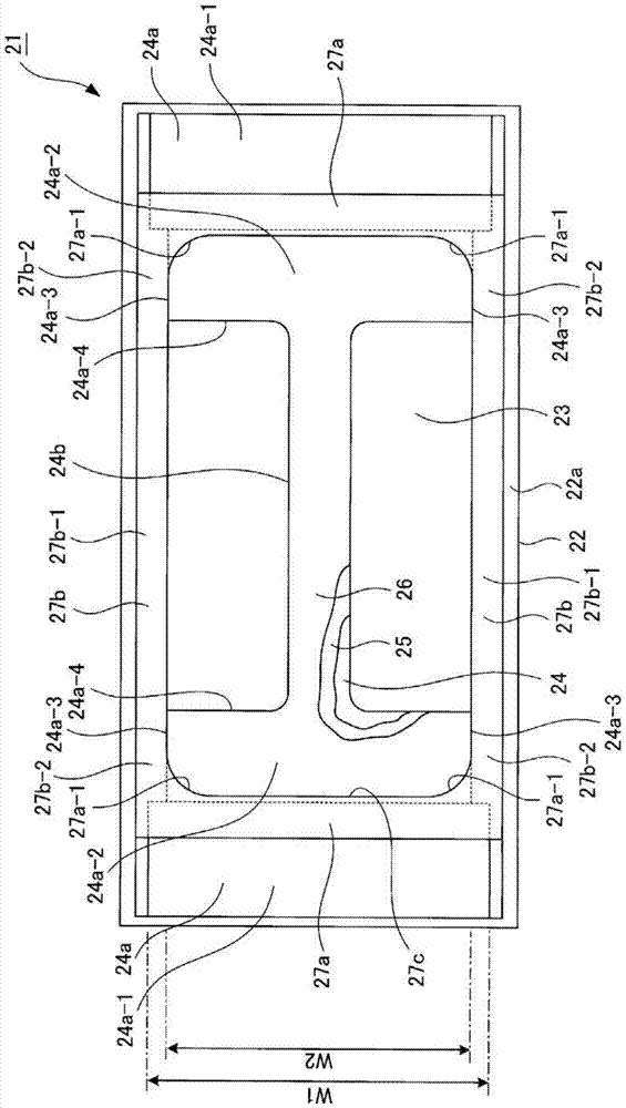
[0091] First, according to Figure 1 ~ Figure 3 The structure of the chip fuse 21 according to the embodiment of the present invention will be described.

[0092] In addition, image 3 Means to remove figure 1 The states of the first protective film 28, the second protective film 29, the mark 30, the end surface electrode 32, and the copper film 33, the nickel film 34, and the tin film 35 on the end surface electrode 32 are shown. In addition, image 3 The fuse element part (fuse link) 24b and the surface electrode part 24a (second electrode part 24a-2) in the nickel film 25 and part of the tin film 26 are broken. Figure 4 In (d), a part of the copper foil 52 is broken. Figure 5 In (a), a part of the copper foil 52 and the photosensitive film 53 is shown to be broken.

[0093] Such as Figure 1 ~ Figure 3 As shown, on the surface 22a of the insulating substrate 22 as an al...


PUM

PropertyMeasurementUnit
electrical resistanceaaaaaaaaaa
thicknessaaaaaaaaaa
electrical resistanceaaaaaaaaaa

Abstract

The present invention provides a chip fuse and a method of manufacturing the chip fuse, and aims at improving the breaking performance such as maintaining the appearance and reducing the continuous arc. In the chip fuse (21), a heat storage layer (23) is formed on an insulating substrate (22), and surface electrode portions (24a) on both sides in the longitudinal direction of the chip fuse are formed on the heat storage layer. ) and the fuse element part (24b) between the above-mentioned surface electrode parts, and a protective film is formed on the fuse element part, wherein, on the heat storage layer in a manner surrounding the fuse element part A rectangular bank (27) is formed on the surface electrode portion, and a first protective film (28) is formed inside the bank. In addition, in the bank forming process, by affixing a sheet-shaped photosensitive group-containing material on the fuse element portion, the surface electrode portion, and the heat storage layer, and attaching the sheet-shaped photosensitive group-containing material Rectangular banks are formed by ultraviolet exposure and development (photolithography).

Description

Technical field [0001] The invention relates to a chip fuse and a method for manufacturing the chip fuse. Background technique [0002] As a component mounted on the surface of a printed wiring board of an electronic device, a chip fuse as a small-sized fuse is conventionally known. The chip fuse is used to prevent the electronic circuit of the printed wiring board from being damaged by overcurrent. [0003] Picture 12 A cross-sectional view of the conventional chip fuse 1 is shown. Such as Picture 12 As shown, a heat storage layer (adhesive layer) 3 is formed on the surface 2a of the insulating substrate 2 as an alumina substrate with epoxy resin, and a copper fuse film 4 is formed on the heat storage layer 3. That is, by providing the heat storage layer 3 between the insulating substrate 2 and the fuse film 4, the fuse film 4 is not in contact with the insulating substrate 2. Therefore, the heat generated by the fuse element portion 4b when the blade fuse 1 is energized is not...

Claims


Application Information

Patent Timeline
Patent Type & Authority Patents(China)
IPC IPC(8): H01H85/02H01H37/76
CPCH01H85/046H01H69/022H01H85/38H01H2069/025H01H2085/383Y10T29/49107H01H85/143H01H69/02H01H85/0013H01H85/48
Inventor 山岸克哉清野英树
Owner KAMAYA ELECTRIC
Why Eureka
Try Eureka