Eight-tube SRAM bit cell circuit working at low voltage suitably and array of eight-tube SRAM bit cell circuit

A bit cell, low-voltage technology, applied in the field of 8-tube SRAM bit cell circuit and its array, can solve the problems of SRAM data competition, non-selected cell data interference, etc., and achieve the effect of eliminating competition and interference

Active Publication Date: 2015-08-05
SUZHOU WULI INFORMATION TECH
View PDF4 Cites 3 Cited by
  • Summary
  • Abstract
  • Description
  • Claims
  • Application Information

AI Technical Summary

Problems solved by technology

[0008] In order to solve the above-mentioned problems in the prior art, the present invention provides an 8-tube SRAM bit cell circuit and its array suitable for low-voltage operation, aiming at solving the problem of data competition during SRAM write operation and the problem of unselected cell data being disturbed

Method used


Image

  • Eight-tube SRAM bit cell circuit working at low voltage suitably and array of eight-tube SRAM bit cell circuit
  • Eight-tube SRAM bit cell circuit working at low voltage suitably and array of eight-tube SRAM bit cell circuit
  • Eight-tube SRAM bit cell circuit working at low voltage suitably and array of eight-tube SRAM bit cell circuit

Examples


Embodiment Construction

[0030] The present invention will be described in detail below with reference to the accompanying drawings and in combination with embodiments.

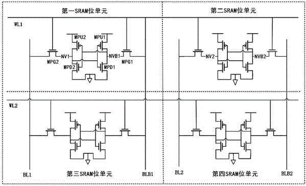
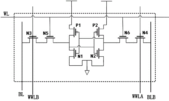
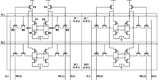
[0031] see figure 2 As shown, an 8-tube SRAM bit cell circuit suitable for low-voltage operation includes a first PMOS transistor P1, a second PMOS transistor P2, a first NMOS transistor N1, a second NMOS transistor N2, a third NMOS transistor N3, and a fourth NMOS transistor. NMOS transistor N4, fifth NMOS transistor N5 and sixth NMOS transistor N6;

[0032] Wherein, the first PMOS transistor P1 and the first NMOS transistor N1 form a first inverter, and the second PMOS transistor P2 and the second NMOS transistor N2 form a second inverter; the first The output terminal of the inverter is directly connected to the input terminal of the second inverter, and the output terminal of the second inverter is directly connected to the input terminal of the first inverter;

[0033] The sources of the first PMOS transistor P1 and the s...


PUM


Abstract

The invention discloses an eight-tube SRAM bit cell circuit working at low voltage suitably and an array of the eight-tube SRAM bit cell circuit. Two NMOS tubes are additionally arranged in a traditional six-tube SRAM bit cell to form the eight-tube SRAM bit cell and are controlled by two signal lines; in the array formed by eight-tube SRAM bit cells, two PMOS tubes are additionally arranged in each column and are controlled by two signal lines; during write operation, the two additional PMOS tubes in each column are controlled to switch off the power supply of each bit cell, the competitive relation is eliminated and no-competition operation is realized; the two control NMOS tubes are additionally arranged in each SRAM bit cell, and the interference to the SRAM bit cells on non-selected columns in the same row in the array can be eliminated; the proposed novel circuit structure can be used for solving the data competition problem and overcoming a defect that non-selected unit data are interfered during write operation of the SRAM, and therefore, a SRAM can work at the lower voltage.

Description

technical field [0001] The invention belongs to the technical field of semiconductor circuits and is used for memory and chip circuit design, in particular to an 8-tube SRAM bit unit circuit suitable for low-voltage operation and an array thereof. Background technique [0002] Such as figure 1 as shown, figure 1 It is a schematic diagram of a traditional 6-tube (6T) SRAM bit cell array. This traditional SRAM array has the following two main disadvantages: [0003] 1. Due to the competition between the data value to be written and the saved data value in the traditional SRAM write operation, the write operation is prone to failure when the voltage is low. [0004] Assume that before the write operation: node NVB1 saves the value "1", and NV1 is "0". [0005] During the write operation, BLB1 is 0, BL1 is 1, and the node NVB1 is pulled down to "0" by the pull-down of BLB1 "0", thus causing the node NV1 to flip to "1". However, in the process of NVB1 being pulled down to "0"...

Claims


Application Information

Patent Timeline
Patent Type & Authority Applications(China)
IPC IPC(8): G11C11/413
Inventor 张建杰张泳培
Owner SUZHOU WULI INFORMATION TECH
Why Eureka
Try Eureka