Transconductance amplifying circuit capable of converting voltage to current

A technology of transconductance amplification and voltage conversion, which is applied to DC-coupled DC amplifiers, differential amplifiers, and improved amplifiers to improve efficiency. The effect of power consumption

Active Publication Date: 2015-08-12
SUZHOU ESIIC TECH CO LTD
View PDF4 Cites 0 Cited by
  • Summary
  • Abstract
  • Description
  • Claims
  • Application Information

AI Technical Summary

Problems solved by technology

The power consumption and performance of the low noise amplifier greatly affect the power consumption and performance of the RF receiving system

Method used

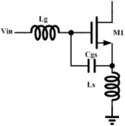
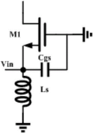

Image

  • Transconductance amplifying circuit capable of converting voltage to current
  • Transconductance amplifying circuit capable of converting voltage to current
  • Transconductance amplifying circuit capable of converting voltage to current

Examples


Embodiment Construction

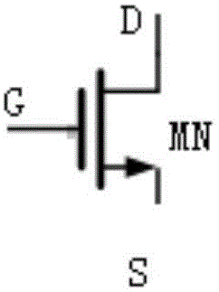
[0030] The principle of this embodiment is to further reduce the power consumption of the amplifier, and propose a new circuit structure in which a single NMOS transistor or a PMOS transistor is replaced by a multi-stage iterative paired NMOS transistor and a PMOS transistor.

[0031] The circuit idea of ​​this embodiment is the first step. A single NMOS transistor or PMOS transistor is replaced by a pair of NMOS transistor and PMOS transistor. Figure 4a and Figure 4b shown.

[0032] In the second step, treat the NMOS transistors or PMOS transistors inside the pair as a single transistor. Instead, use pairs of NMOS and PMOS transistors, see Figure 4c shown.

[0033] In the third step, each NMOS transistor or PMOS transistor in the circuit after one iteration can be further regarded as a single transistor, and replaced by a pair of NMOS transistors and PMOS transistors.

[0034] In the fourth step, repeat the third step until other limitations of the circuit stop, such a...


PUM


Abstract

The application discloses a transconductance amplifying circuit capable of converting voltage to current, specifically a circuit which uses layers of N type transistors and P type transistors, which are paired, to replace single N type transistor (NMOS transistor) and single P type transistor (PMOS transistor). The replaced N type transistors and the P type transistors, which are paired, have identical transconductance, but the consumed current and power dissipation are reduced. The circuit of the application belongs to the technical field of an integrated circuit. The circuit of the invention is low in power dissipation and can be widely applied to a transconductance generating circuit of a radio frequency analog circuit.

Description

technical field [0001] The invention relates to the fields of integrated circuit design and signal processing, in particular to a transconductance amplifying circuit for converting voltage into current. Background technique [0002] In radio frequency microwave communication, the input radio frequency signal needs to be amplified by a low noise amplifier, then mixed down to a low frequency by a local oscillator signal, then amplified by a low frequency amplifier, frequency selected by a filter, and then passed through a mode The digital converter (ADC) is handed over to the baseband for processing. Therefore, the low noise amplifier is the key circuit of the radio frequency receiving system. The power consumption and performance of the low noise amplifier greatly affect the power consumption and performance of the radio frequency receiving system. [0003] In the existing integrated circuit design, the current and power consumption of the chip are required to be as low as ...

Claims


Application Information

Patent Timeline
IPC IPC(8): H03F1/02H03F1/26H03F3/45
Inventor 樊晓华
Owner SUZHOU ESIIC TECH CO LTD
Why Eureka
Try Eureka