
Gas-liquid two-phase atomization cleaning device and cleaning method

An atomization cleaning and gas-liquid technology, applied in liquid cleaning methods, chemical instruments and methods, cleaning methods and utensils, etc., can solve the problems of wafer surface graphic structure damage, low utilization rate of liquid phase fluid, waste of resources, etc. , to achieve the effect of improving cleaning effect, preventing damage and saving liquid phase fluid

Active Publication Date: 2015-08-19
BEIJING SEVENSTAR ELECTRONICS CO LTD
View PDF6 Cites 19 Cited by
  • Summary
  • Abstract
  • Description
  • Claims
  • Application Information

AI Technical Summary

Problems solved by technology

[0004] However, with the further reduction of the feature size of the pattern structure on the wafer surface, the high-speed jet liquid phase fluid will cause serious damage to the pattern structure of the wafer surface.
Large-sized liquid-phase particles or liquid-phase jets generally exist in the traditional cleaning spray technology, which seriously damages the surface patterns of 65nm and below process wafers. At the same time, the utilization rate of liquid-phase fluid is low, resulting in an extreme waste of resources.

Method used


Image

  • Gas-liquid two-phase atomization cleaning device and cleaning method
  • Gas-liquid two-phase atomization cleaning device and cleaning method
  • Gas-liquid two-phase atomization cleaning device and cleaning method

Examples


Embodiment Construction

[0035] In order to make the content of the present invention clearer and easier to understand, the content of the present invention will be further described below in conjunction with the accompanying drawings. Of course, the present invention is not limited to this specific embodiment, and general replacements known to those skilled in the art are also covered within the protection scope of the present invention. Secondly, the present invention is described in detail by means of schematic diagrams. When describing the examples of the present invention in detail, for the convenience of explanation, the schematic diagrams are not partially enlarged according to the general scale, which should not be used as a limitation of the present invention.

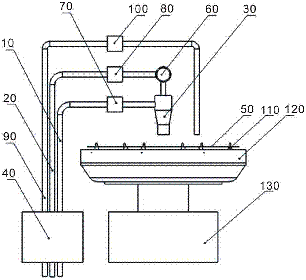
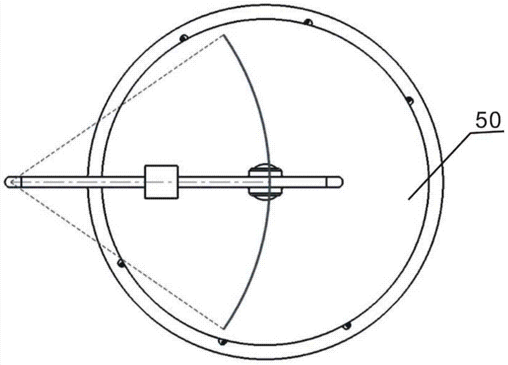
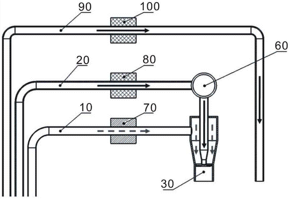
[0036] It should be noted that, in the following examples, using Figure 1-9 The schematic diagram of the structure describes in detail the gas-liquid two-phase atomization cleaning device according to the present invention. When des...


PUM

PropertyMeasurementUnit
Diameteraaaaaaaaaa

Abstract

The invention provides a gas-liquid two-phase atomization cleaning device and relates to the technical field of the semiconductor chip technology. The gas-liquid two-phase atomization cleaning device comprises a gas pipeline, a liquid pipeline and a gas-liquid two-phase atomization nozzle, one end of the gas pipeline and one end of the liquid pipeline are arranged on a swing arm while the other end of the gas pipeline and the other end of the liquid pipeline are communicated with the gas-liquid two-phase atomization nozzle to form atomization particles, and the swing arm drives the gas-liquid two-phase nozzle to reciprocate in a circular arc manner between the edge and the center of a wafer. High-speed liquid flow and high-speed gas flow are sufficiently acted through a gas-liquid two-phase atomization nozzle structure, superfine atomized droplets uniform in particle size are formed by adjusting gas flow rate and liquid flow rate of small flow rate, the superfine atomized droplets are sprayed on the surface of the wafer after being accelerated through the high-speed gas flow, and cleaning is completed. By the arrangement, transferring of impurities in troughs to a main flow body is promoted, efficiency in cleaning is improved, cleaning effect is improved, and damage to the surface structure of the wafer is reduced due to small quality of the atomization particles.

Description

technical field [0001] The invention belongs to the technical field of semiconductor wafer technology, and specifically relates to a gas-liquid two-phase atomization cleaning device and a cleaning method. Background technique [0002] As the feature size of integrated circuits enters the deep sub-micron stage, the cleanliness of the wafer surface required in the integrated circuit wafer manufacturing process is becoming more and more stringent. In order to ensure the cleanliness of the wafer material surface, there are several Hundreds of cleaning processes, the cleaning process accounts for 30% of the entire manufacturing process. [0003] In the semiconductor cleaning process, when the cleaning liquid impacts the wafer at a high speed, it will generate a physical force on the wafer, which can accelerate the process of cleaning the chemical liquid and impurities and pollutants on the surface of the wafer, and promote impurities and pollution. The substance is corroded by t...

Claims


Application Information

Patent Timeline
IPC IPC(8): B08B3/02B08B13/00
CPCB08B3/022B08B13/00B08B2203/02
Inventor 滕宇吴仪
Owner BEIJING SEVENSTAR ELECTRONICS CO LTD
Learn More