
Device for measuring subsurface structure characteristic and micro-area wideband dielectric property

A technology of dielectric properties and structural features, applied in the field of subsurface structure imaging of nanocomposite material systems and measurement devices for micro-area broadband dielectric properties, can solve the lack of spatial resolution, technology and Unsuitable analytical methods, uneven dispersion of nanoparticles, etc.

Inactive Publication Date: 2015-08-19
THE NAT CENT FOR NANOSCI & TECH NCNST OF CHINA
View PDF4 Cites 18 Cited by
  • Summary
  • Abstract
  • Description
  • Claims
  • Application Information

AI Technical Summary

Problems solved by technology

For example, for a particle dispersion system with a radius of about 100nm, some current mature theories can be used to analyze the dielectric spectrum, but for a heterogeneous dispersion system of nanoparticles smaller than 100nm, the current macroscopic technology and analysis methods are not suitable.
[0011] A basic defect of existing dielectric spectroscopy techniques is the lack of spatial resolution for heterogeneous systems or nano-dispersed structures

Method used


Image

  • Device for measuring subsurface structure characteristic and micro-area wideband dielectric property
  • Device for measuring subsurface structure characteristic and micro-area wideband dielectric property
  • Device for measuring subsurface structure characteristic and micro-area wideband dielectric property

Examples


Embodiment Construction

[0022] Specific embodiments of the present invention will be described in detail below in conjunction with the accompanying drawings. It should be understood that the specific embodiments described here are only used to illustrate and explain the present invention, and are not intended to limit the present invention.

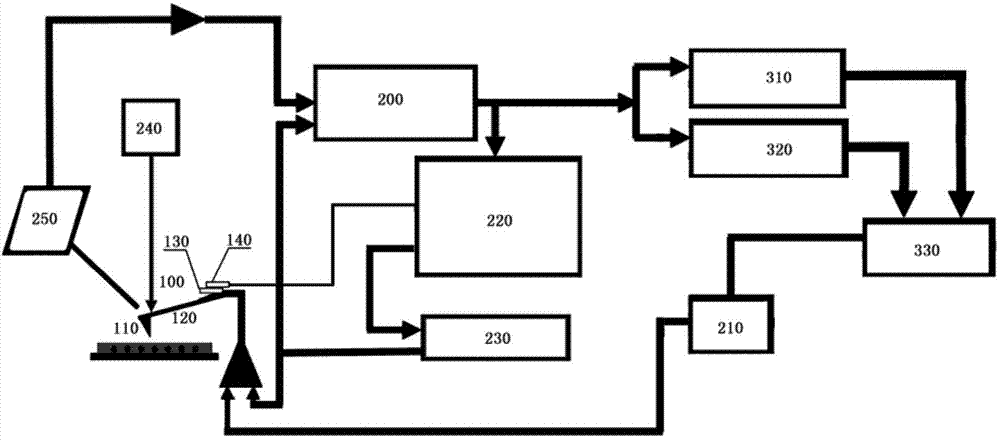
[0023] Such as figure 1 As shown, according to one embodiment of the present invention, a kind of subsurface structure characteristic based on electrostatic force microscope and the measuring device of micro-region broadband dielectric properties are provided, including:

[0024] Electrostatic force microscope, which includes:

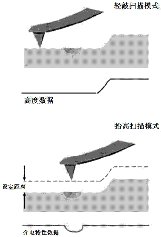
[0025] The conductive micro-cantilever probe 100 includes a conductive probe part 110 and a micro-cantilever part 120, and the conductive micro-cantilever probe 100 is used to scan the sample to be tested for the first time in the tapping scanning mode;

[0026] The lock-in amplifier 200 is used to receive the reference frequency signa...


PUM


Abstract

The invention discloses a device for measuring subsurface structure characteristic and micro-area wideband dielectric property, and the device comprises an electrostatic force microscope which comprises a conductive miniature cantilever probe comprising a conductive probe part and a miniature cantilever probe part, wherein a probe carries out the first scanning of a to-be-measured sample in a touch scanning mode. The device also comprises a phase-locking amplifier which is used for receiving a reference frequency signal and a real-time signal generated in the first scanning process, and generating a first phase signal according to the reference frequency signal and the real-time signal. After the first scanning, the probe carries out the second scanning of the to-be-measured sample along the scanning trace of the first scanning in a mode of lifted scanning. The phase-locking amplifier also generates a second phase signal according to the reference frequency signal and a real-time signal generated in the second scanning process. The device also comprises a signal source which enables a modulation voltage signal to be applied to the conductive probe part in the second scanning process, and to be outputted to an external phase-locking amplifier. The device also comprises the external phase-locking amplifier which is used for receiving the modulation voltage signal and the second phase signal, and obtaining a dielectric response signal and a dielectric loss angle signal according to the modulation voltage signal and the second phase signal.

Description

technical field [0001] The invention relates to a measuring device for subsurface structure characteristics and micro-area broadband dielectric properties based on an electrostatic force microscope, in particular to a measuring device for nano-composite material system sub-surface structure imaging and micro-area broadband dielectric properties. Background technique [0002] Broadband dielectric spectroscopy (BDS) technology is a field of great interest in recent years. Due to its simple and rapid measurement, wide measurement frequency, and non-destructive in-situ detection, it is widely used in polymer materials, biomedicine, and food. , Power engineering and other fields have developed very rapidly. The so-called dielectric spectrum, in engineering, generally refers to the regular change of the permittivity and dielectric loss factor of the dielectric material under the action of the external electric field with the frequency of the applied electric field and the change o...

Claims


Application Information

Patent Timeline
IPC IPC(8): G01Q60/00
Inventor 张冬冬王小伟王锐裘晓辉
Owner THE NAT CENT FOR NANOSCI & TECH NCNST OF CHINA
Learn More