Array substrate and restoration method, test method and manufacture method thereof, and display apparatus

An array substrate and substrate technology, applied in static indicators, semiconductor/solid-state device manufacturing, organic semiconductor devices, etc., can solve problems such as black lines on the display screen, complex production processes, and the inability to quickly and easily repair data line breaks, etc., to achieve The repair process is simple and easy to achieve

Inactive Publication Date: 2015-08-19
HEFEI XINSHENG OPTOELECTRONICS TECH CO LTD +1
View PDF8 Cites 10 Cited by
  • Summary
  • Abstract
  • Description
  • Claims
  • Application Information

AI Technical Summary

Problems solved by technology

In the production process of the array substrate, due to the complex production process, the data line may be disconnected due to the influence of the production process or the factory environment, which will cause black lines in the display screen and seriously affect the display quality of the screen.
The array substrate structure and repair process in the prior art cannot realize fast and simple repair of defects such as data line disconnection

Method used


Image

  • Array substrate and restoration method, test method and manufacture method thereof, and display apparatus
  • Array substrate and restoration method, test method and manufacture method thereof, and display apparatus
  • Array substrate and restoration method, test method and manufacture method thereof, and display apparatus

Examples


Embodiment 1

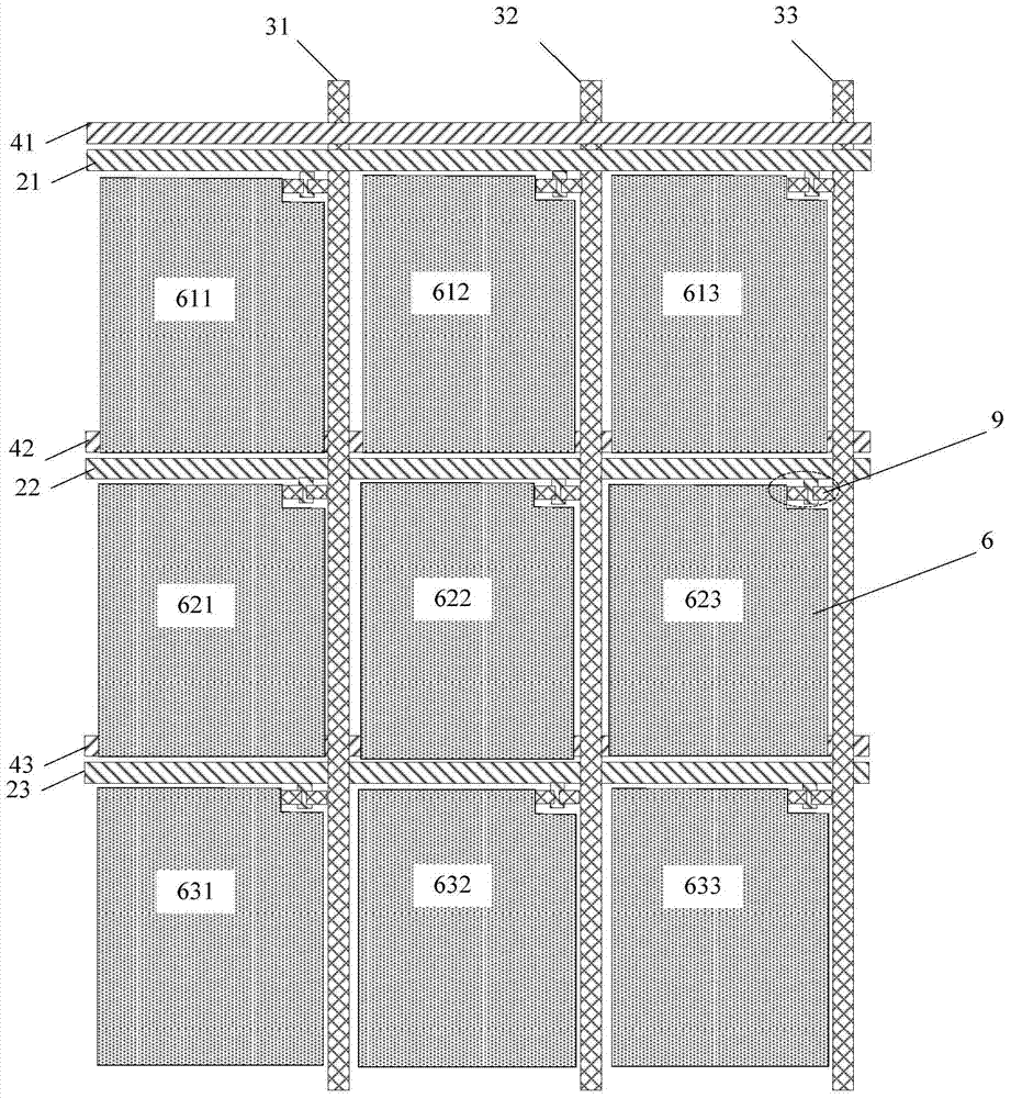
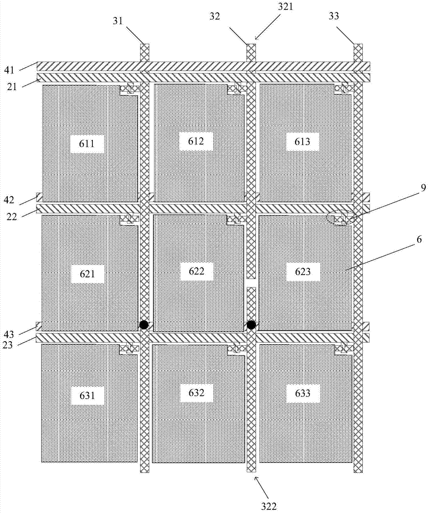
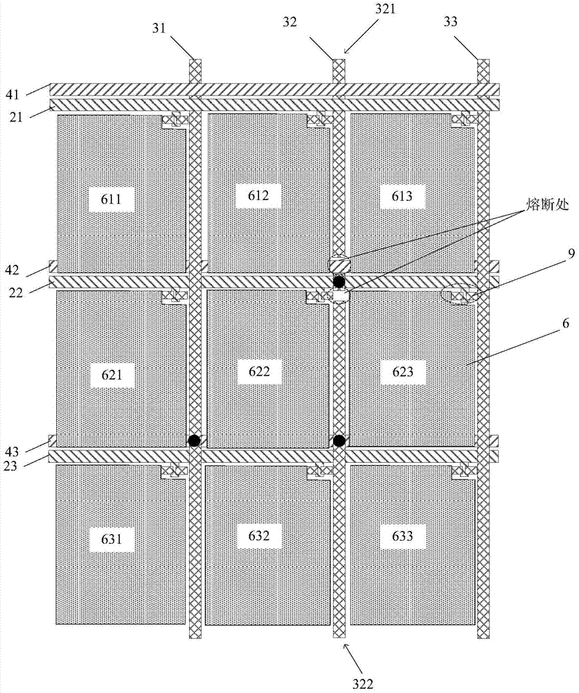
[0033] Embodiment 1 of the present invention provides the structure of the array substrate, which can be referred to figure 1 and 4 , including: base1( figure 1 Not shown in ), the gate line pattern and data line pattern formed on the substrate 1, each row of gate lines 21, 22, 23 in the gate line pattern and each column of data lines 31, 32, 33 in the data line pattern perpendicularly intersect , dividing the array substrate into a plurality of pixels, and further including a spare line pattern formed on the same layer as the gate line pattern, the spare line pattern including a plurality of spare lines 41, 42, 43 parallel to the gate lines in the gate line pattern, A spare line is formed at the position of each row of pixels, and there is a vertical overlapping area between the spare line and the data line connected to each pixel in the row. In addition, a gate insulating layer 5 for isolating the gate line pattern, the spare line pattern and the data line pattern is also ...

Embodiment 2

[0044] In the H-ADS array substrate in the prior art, since the pixel electrodes are fabricated under the common electrode layer, the test terminals cannot be connected to the pixel electrodes, and corresponding electrical performance tests cannot be realized. In order to overcome such problems, Embodiment 2 of the present invention provides a new type of H-ADS array substrate.

[0045] refer to Figure 5 and 6 As shown, the array substrate provided in Embodiment 2 is an H-ADS (High Aperture Ratio Edge Field Switching) substrate. Compared with the array substrate provided in Embodiment 1, it also includes: a passivation layer formed on the pixel electrode pattern Pattern 7 and the common electrode pattern 8 formed on the passivation layer pattern 7; each spare line pattern has a vertical overlapping area with the pixel electrode block above it, and the passivation layer pattern 7 is formed at a position corresponding to the vertical overlapping area There is a positioning ho...


PUM


Abstract

The invention provides an array substrate and a restoration method, test method and manufacture method thereof, and a display apparatus. The array substrate comprises a substrate, a grid wire figure and a data line figure which are formed on the substrate, and a gate insulation layer formed between the grid wire figure and the data line figure, and further comprises a spare line figure formed at the same layer as the grid wire figure. The spare line figure comprises multiple spare lines parallel to grid wires in the grid wire figure, and the spare lines are distributed at positions of multiple rows of pixels which are limited by the grid wire figure and the data line figure and form vertical overlapping areas with data lines in the data line figure. The array substrate and the restoration method thereof, provided by the invention, when the array substrate generates a data line circuit break defect, can rapidly restore the defect. Besides, the restoration process is simple, and the realization is easy.

Description

technical field [0001] The present invention relates to the field of display technology, in particular to an array substrate and its repair method, testing method, manufacturing method, and display device. Background technique [0002] With the development of display manufacturing technology, liquid crystal display technology has developed rapidly, and has replaced traditional picture tube displays and become the mainstream of future flat panel displays. In the field of liquid crystal display technology, TFT-LCD (Thin Film Transistor Liquid Crystal Display) is widely used in televisions, computers, and mobile phones due to its large size, high integration, powerful functions, flexible process, and low cost. machines and other fields. [0003] The display panel is the main part of TFT-LCD. It is generally assembled from the completed array substrate and color filter substrate and filled with liquid crystals. The array substrate includes a number of gate lines and data lines....

Claims


Application Information

Patent Timeline
Patent Type & Authority Applications(China)
IPC IPC(8): G09G3/36G02F1/1343G02F1/1362
CPCG09G3/3648G09G2330/08G02F1/136259G02F1/136263G02F1/136272H01L21/76894H01L27/1244G02F2201/506G02F2201/508G09G2330/12H10K71/861G02F1/13
Inventor 冯伟
Owner HEFEI XINSHENG OPTOELECTRONICS TECH CO LTD
Why Eureka
Try Eureka