Accuracy reconfigurable delay line ADC circuit for digital power supply
A technology of analog-to-digital converter and digital power supply, which is applied in the direction of analog-to-digital converters, etc. It can solve the problems of high power consumption waste and insufficient voltage precision, so as to reduce power consumption, meet the requirements of power consumption and precision, and meet high-precision required effect
- Summary
- Abstract
- Description
- Claims
- Application Information
AI Technical Summary
Problems solved by technology
Method used
Image

Examples
Embodiment
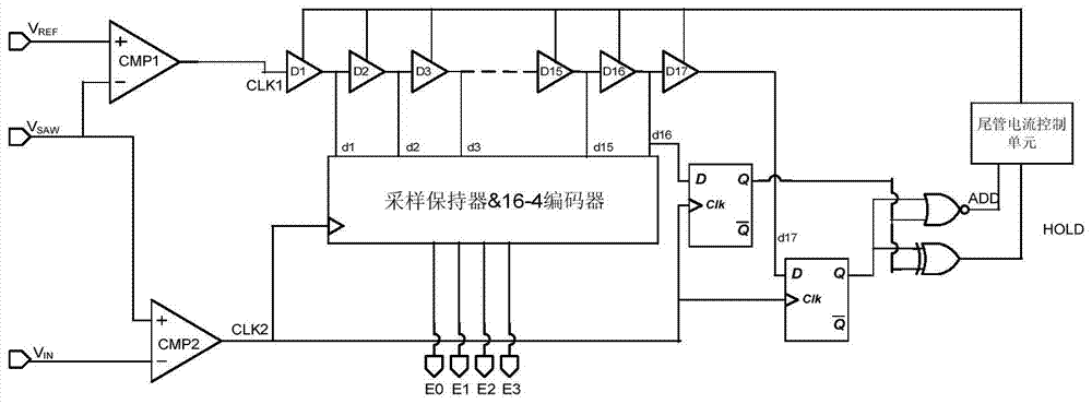
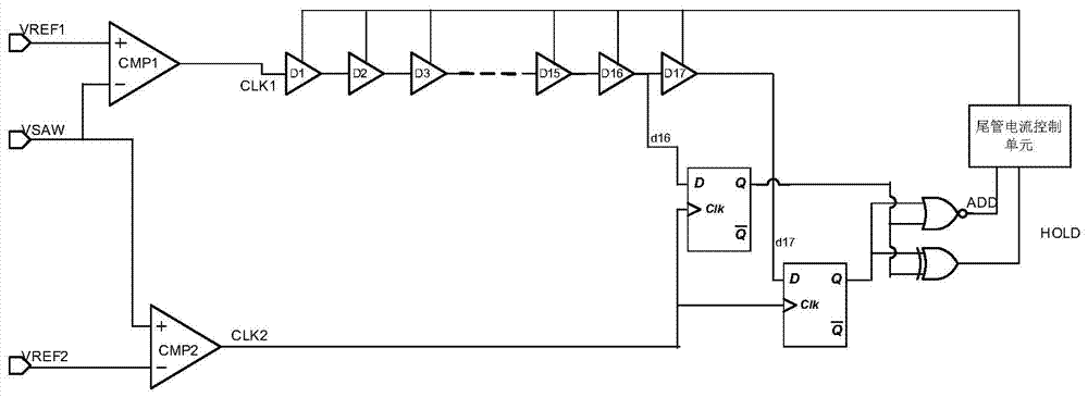
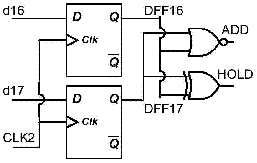
[0040] figure 1 A block diagram of a 4-bit delay line analog-to-digital converter. The working process is divided into two parts: calibration and quantification. figure 2 Schematic diagram of the operation of the calibration portion of the 4-bit delay line ADC. In an ideal situation, the signal is sequentially transmitted from the 1st delay unit to the 17th delay unit. After the signal passes through the nth delay unit, it is dn, and each time it passes through a delay unit, the delay time is t d , then the total delay time after 16 delay units is 16t d . In order for the analog-to-digital converter to accurately quantify the input voltage, it is necessary to ensure that the signal is just transmitted from the first delay unit to the 17th delay unit within one clock cycle, that is, to satisfy 16t d equal to the length of one clock cycle T D .
[0041] In order to ensure that the delay unit can maintain the correct delay time under different processes, power supply volt...
PUM
 Abstract
Description
Claims
Application Information
PatSnap Eureka turns technology decisions into work you can execute. Powered by our Innovation Knowledge Graph, it runs expert workflows across engineering, life sciences, materials and intellectual property. Get your review-ready output in minutes.


