Polymer film circuit board and electronic component interconnection method

A technology of electronic components and polymer films, which is applied in the manufacture of electrical components, printed circuits, printed circuits, etc., can solve the problems of low glass transition temperature and achieve the effects of short assembly time, simple and reliable process, and small volume

Inactive Publication Date: 2015-08-19
TIANJIN UNIV
View PDF4 Cites 7 Cited by
  • Summary
  • Abstract
  • Description
  • Claims
  • Application Information

AI Technical Summary

Problems solved by technology

Due to the low glass transition temperature of commonly used engineering thermoplastic polymers, the packaging of surface mount devices (SMD) is not suitable for traditional processes such as wire bonding and reflow soldering

Method used


Image

  • Polymer film circuit board and electronic component interconnection method

Examples


Embodiment Construction

[0022] The present invention will be further described below in conjunction with the accompanying drawings.

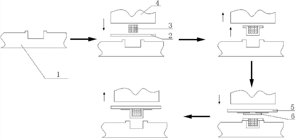
[0023] Such as figure 1 Shown: a kind of polymer film circuit board and the interconnection method of electronic components and parts, it is characterized in that, comprises the following steps:

[0024] (1) Design and process the concave mold 1 for placing the electronic components 3 according to the external dimensions of the electronic components; The mold 1 is made of metal material and processed by tools such as machine tools.

[0025] (2) Place a layer of polymer film 2 above the concave mold 1, place the electronic components 3 on the polymer film 2, and align with the groove of the concave mold 1, wherein the electronic components 3 The surface with metal connection pins is placed outwards, and the size of the concave mold 1 should be the sum of the outline size of the electronic component 3 and the thickness of the polymer film 2 used for packaging.

[0026...


PUM


Abstract

The invention discloses a polymer film circuit board and electronic component interconnection method comprising the following steps: (1) processing a concave mold according to the size of an electronic component; (2) placing a polymer film above the concave mold, and placing the electronic component on the polymer film; (3) pressing the electronic component into the groove of the concave mold by an ultrasonic embossing welding method; (4) taking the electronic component packaged with the polymer film out from the concave mold, cutting off the excess part of the polymer film, and putting the electronic component packaged with the polymer film into the concave mold again; (5) laying a conductive film; and (6) heating and welding the polymer film packaging the electronic component and a polymer film on a circuit board together by an ultrasonic embossing welding technology. According to the method, a conductive film and an embossing process are combined to realize electrical connection between an SMD and a circuit board and fixation of the SMD.

Description

technical field [0001] The invention relates to a method for connecting circuit boards and electronic components, more specifically, to a method for interconnecting polymer film circuit boards and electronic components. Background technique [0002] Due to the low glass transition temperature of thermoplastic polymers, surface microstructure processing can be realized by hot embossing process. Polymer microdevices are widely used in optical devices, microfluidic chips and other fields. On polymer microdevices Realizing the integration of microstructure and electricity is the development trend of micro-optical (hydraulic) electromechanical devices in the future. Due to the low glass transition temperature of commonly used engineering thermoplastic polymers, surface mount device (SMD) packaging is not suitable for traditional processes such as wire bonding and reflow soldering. Contents of the invention [0003] The purpose of the present invention is to overcome the defici...

Claims


Application Information

Patent Timeline
Patent Type & Authority Applications(China)
IPC IPC(8): H05K3/34
CPCH05K3/341H05K2203/0285
Inventor 崔良玉田延岭张大为
Owner TIANJIN UNIV
Why Eureka
Try Eureka