Supercharge Your Innovation With Domain-Expert AI Agents!

Masking plate assembly, display device and manufacturing method

A manufacturing method and mask technology, which can be applied to devices for coating liquid on the surface, semiconductor/solid-state device manufacturing, electrical components, etc., and can solve problems affecting mask bonding, uneven mask surface, and shadows. effect and other issues to achieve the effect of improving the display effect

Active Publication Date: 2015-08-26
BOE TECH GRP CO LTD
View PDF3 Cites 4 Cited by
  • Summary
  • Abstract
  • Description
  • Claims
  • Application Information

AI Technical Summary

Problems solved by technology

During the removal process, the edge of the mask will warp due to stress, and the warping will affect the adhesion of the mask to the substrate during the evaporation process, so shadow effects will appear near the edge of the formed pixel area
In addition, during the welding process, there will be left figure 1 The solder joints 31 shown, the solder joints 31 will also cause unevenness on the surface of the mask plate

Method used


Image

  • Masking plate assembly, display device and manufacturing method
  • Masking plate assembly, display device and manufacturing method
  • Masking plate assembly, display device and manufacturing method

Examples


Embodiment Construction

[0028] In order to make the technical problems, technical solutions and advantages to be solved by the present invention clearer, the following will describe in detail with reference to the drawings and specific embodiments.

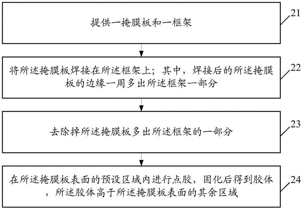
[0029] In order to avoid the phenomenon of unevenness on the surface of the mask plate, the embodiment of the present invention provides a new manufacturing method of the mask plate assembly, such as figure 2 shown, including:

[0030] Step 21, providing a mask plate and a frame;

[0031] Step 22, welding the mask plate on the frame; wherein, the welded mask plate has redundant parts beyond the frame;

[0032] Step 23, removing at least a part of the redundant parts;

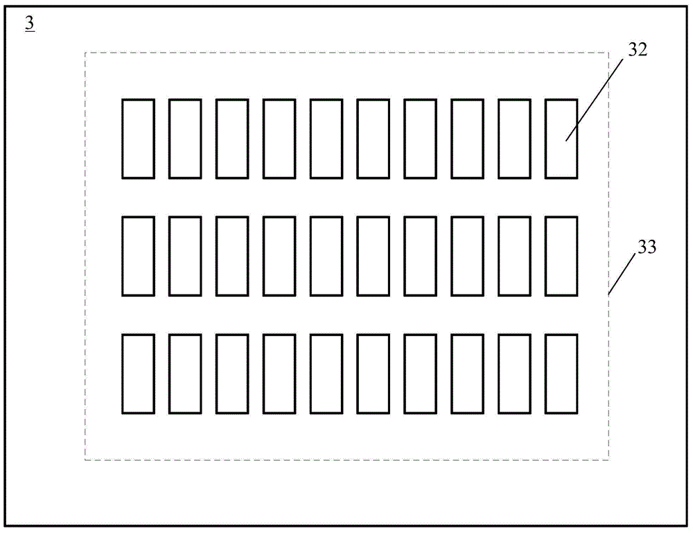
[0033] Step 24, dispensing glue in a preset area on the surface of the mask, and obtaining a colloid after curing, the colloid being higher than the remaining areas on the surface of the mask.

[0034] In the manufacturing method of this embodiment, the mask plate is indirectly bonded ...


PUM


Abstract

The invention provides a masking plate assembly, a display device and a manufacturing method, belonging to the field of displaying of organic light-emitting diodes. The manufacturing method for the masking plate assembly comprises the following steps: providing a masking plate and a framework; welding the masking plate on the framework, wherein the welded masking plate has unwanted parts beyond the framework; removing at least a part of the unwanted parts; and carrying out dispensing in a preset area on the surface of the masking plate and carrying out curing so as to obtain colloid, wherein the colloid is higher than the rest area of the surface of the masking plate. According to the invention, the colloid formed on the surface of the masking plate is bonded with a substrate, so more smooth bonding effect is guaranteed, and vapor deposition quality is consequently improved.

Description

technical field [0001] The invention relates to an organic light emitting diode display, in particular to a mask plate component, a display device and a manufacturing method. Background technique [0002] Organic Light Emitting Diode (OLED) display is recognized by the industry as the second largest display after Liquid Crystal Display (LCD) due to its thinness, active light emission, fast response speed, wide viewing angle, rich colors and high brightness, low power consumption, high and low temperature resistance and many other advantages. The third-generation display technology can be widely used in terminal products such as smartphones, tablets, and TVs. [0003] At present, in the production process of OLED, a fine metal mask (FMM) is used for vapor deposition to form a film layer on the substrate. Such as figure 1 As shown, a fine metal mask (FMM) mainly includes a frame 2 (Frame) and a mask 3 . The mask plate is welded on the Frame. Generally, the length of the mas...

Claims


Application Information

Patent Timeline
IPC IPC(8): C23C14/04H01L51/56
CPCC23C14/042H10K71/166B29C66/472B29C66/324B29C65/7855H10K71/00B05D7/14
Inventor 张粲梁逸南
Owner BOE TECH GRP CO LTD
Features
  • R&D
  • Intellectual Property
  • Life Sciences
  • Materials
  • Tech Scout
  • Unparalleled Data Quality
  • Higher Quality Content
  • 60% Fewer Hallucinations
Learn More