Multiscale modeling and detection method for photoelectric conversion efficiency of plasmonic devices

A photoelectric conversion efficiency, plasma technology, applied in the field of nanophotonics

Active Publication Date: 2017-09-26
BEIJING COMPUTATIONAL SCI RES CENT
View PDF3 Cites 0 Cited by
  • Summary
  • Abstract
  • Description
  • Claims
  • Application Information

AI Technical Summary

Problems solved by technology

[0005] Aiming at the problems existing in the existing surface plasmon modeling and simulation calculations, the purpose of the present invention is to provide a multi-scale modeling and detection method for the photoelectric conversion efficiency of plasma devices

Method used


Image

  • Multiscale modeling and detection method for photoelectric conversion efficiency of plasmonic devices
  • Multiscale modeling and detection method for photoelectric conversion efficiency of plasmonic devices
  • Multiscale modeling and detection method for photoelectric conversion efficiency of plasmonic devices

Examples


Embodiment Construction

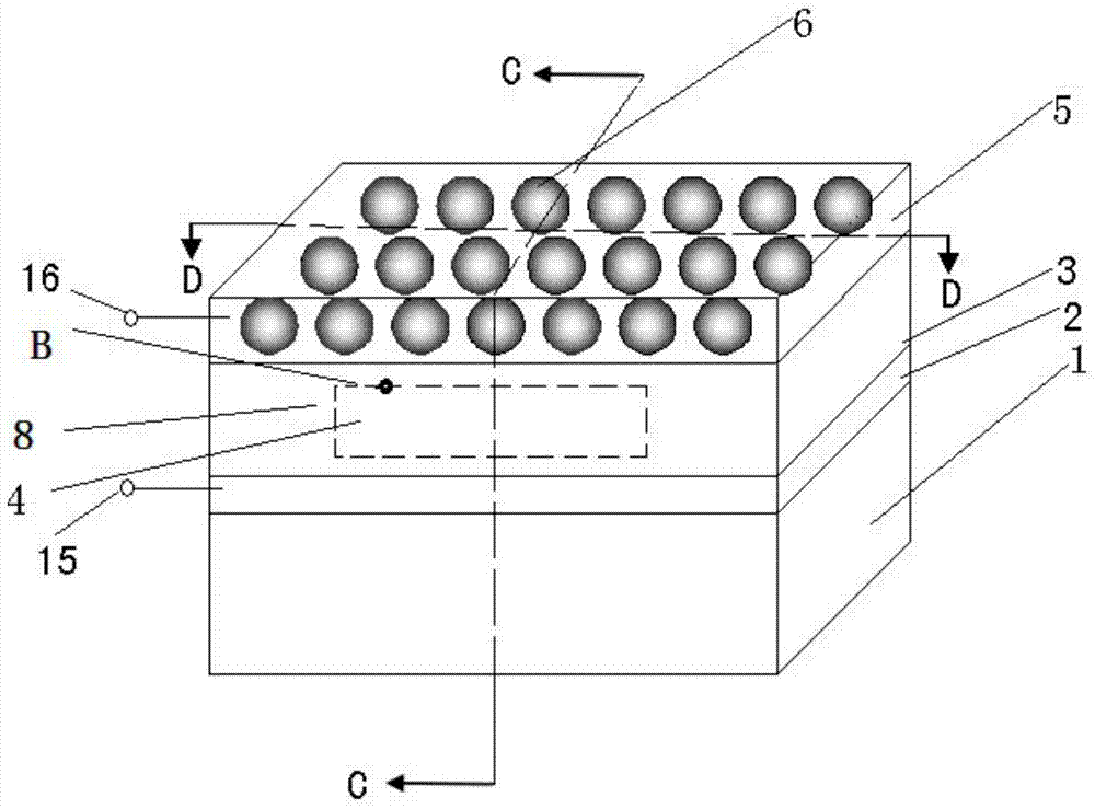
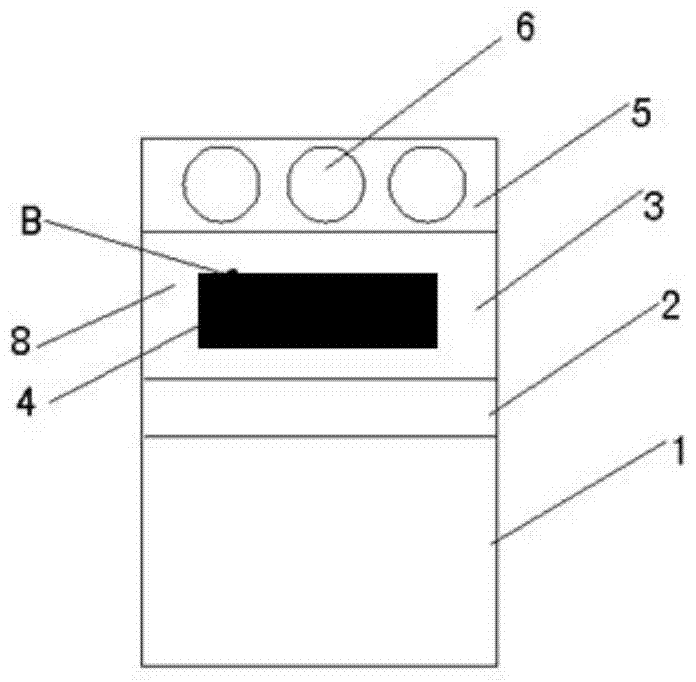
[0046] Such as figure 1 and figure 2 As shown, the plasma device of the present invention includes a substrate 1, a first electrode 2 located on the substrate, a semiconductor component 3 and a second electrode 5 located on the first electrode 2, and a semiconductor component 3 and a second electrode sandwiched between the semiconductor component 3 and the second electrode 5. A metal nanoparticle layer 6 between the electrodes 5. Wherein, the semiconductor component 3 includes a first semiconductor 4 shown by a dotted line in its central area and a second semiconductor 8 surrounding the first semiconductor 4, and the first semiconductor 4 and the second semiconductor 8 are integrally formed.

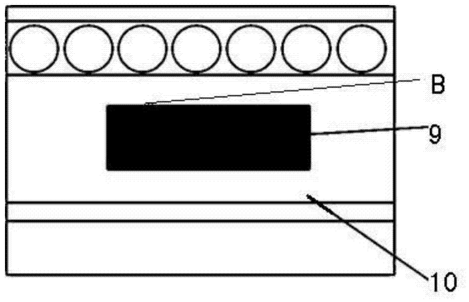
[0047] Such as image 3 and Figure 4 As shown, the plasmonic device of the present invention includes two regions, namely, a quantum region 9 filled with black and a classical region 10 not filled with black. The quantum region 9 includes a first semiconductor 4, the classical regi...


PUM


Abstract

A multi-scale modeling and detecting method for the photoelectric conversion efficiency of a plasma device comprises the following steps: dividing the plasma device into a quantum area and a classic area, wherein the quantum area comprises a first semiconductor, and the classic area comprises a substrate, a metal nanometer granular layer, a first electrode, a second electrode and a second semiconductor; applying bias voltage to the first electrode and the second electrode, and exciting plasmon polaritons of the metal nanometer granular layer through incident light, so as to achieve electric field strengthening effect under the excitation of the plasmon polaritons in the quantum area; during the excitation of the plasmon polaritons, performing classical electrodynamic analysis in the classic area to obtain the electrical potential distribution of the quantum area scattered by the metal nanometer granular layer, obtaining the optical excitation and transportation process of electrons by utilizing quantum mechanics, and obtaining the electric current of the plasma device through the self-consistency, so as to further obtain the photoelectric conversion efficiency. According to the invention, the precision of the quantum mechanics and the high efficiency of the electromagnetism are combined to realize the precise detection of the photoelectric conversion efficiency of the plasma device.

Description

technical field [0001] The invention relates to the field of nanophotonics, in particular to a multi-scale modeling and detection method for photoelectric conversion efficiency of plasma devices. Background technique [0002] Surface plasmon photonics (Plasmonics) is a new subject that has developed rapidly in recent years by applying surface plasmon technology to the field of photonics. It is the most important part of nanophotonics. Surface plasmon photonics encompasses a very wide range of applications such as electric field enhancement, surface-enhanced spectroscopy, enhanced light transmission, surface plasmon nanowaveguides, solar panels, surface plasmon resonance sensors, surface-enhanced energy transfer, and selective light absorption etc. [0003] Surface plasmon is a wave propagating along the surface of a conductor. When the surface structure of a metal is changed, the properties, dispersion relations, excitation modes, and coupling effects of surface plasmon pol...

Claims


Application Information

Patent Timeline
Patent Type & Authority Patents(China)
IPC IPC(8): G06F17/50G06T17/30H02S50/10
CPCY02E10/50
Inventor 任志勇陈冠华孟令一
Owner BEIJING COMPUTATIONAL SCI RES CENT
Why Eureka
Try Eureka