Method for preventing thin film at edge of silicon chip from being peeled off

A thin-film stripping and silicon nitride thin-film technology, applied in electrical components, electrical solid-state devices, semiconductor/solid-state device manufacturing, etc., can solve problems such as brittleness and stripping, eliminate potential risks, and solve the problem of thin film stripping at the edge of silicon wafers. Effect

Inactive Publication Date: 2015-08-26
WUHAN XINXIN SEMICON MFG CO LTD
View PDF5 Cites 6 Cited by
  • Summary
  • Abstract
  • Description
  • Claims
  • Application Information

AI Technical Summary

Problems solved by technology

[0003] Due to the deposition of a thicker film, the stress of the deposited film does not match the substrate silicon wafer, which usually produces a large stress, which leads to a certain degree of warping of the silicon wafer; due to the need for etching with a high aspect ratio, In order to prevent the photoresist from dumping, it is usually necessary to deposit a hard mask layer with a certain thickness, and the hard mask layer commonly used at present, such as amorphous carbon and other thin films, is relatively brittle, and it is easy to deposit on silicon wafers with a high degree of warpage. Delamination of the film occurs at the edge

Method used


Image

  • Method for preventing thin film at edge of silicon chip from being peeled off
  • Method for preventing thin film at edge of silicon chip from being peeled off
  • Method for preventing thin film at edge of silicon chip from being peeled off

Examples


Embodiment Construction

[0024] In order to make the technical solutions and advantages of the present invention more comprehensible, further details will be described below in conjunction with the accompanying drawings. It should be noted that the specific embodiments described here are only used to explain the present invention, not to limit the present invention.
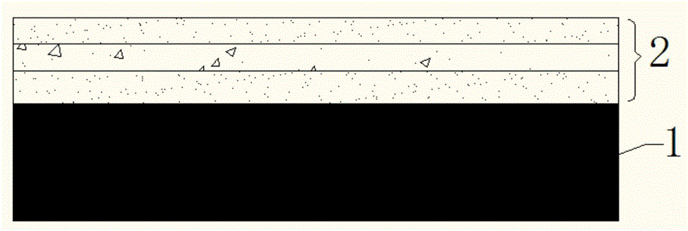
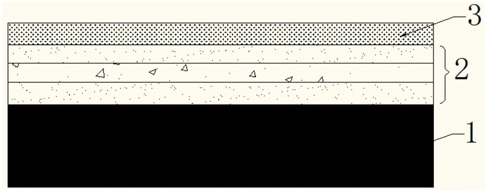
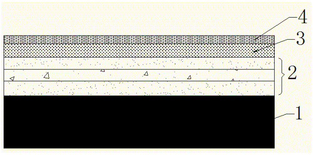
[0025] The core idea of ​​the present invention is: when using the existing process flow, due to the large degree of warpage of the silicon wafer, in the process of depositing the amorphous carbon film, due to the brittle nature of the film, it is easy to be damaged during the cooling process of the silicon wafer. The phenomenon that the edge of the silicon wafer is peeled off. And adopt the method of the present invention, before depositing the amorphous carbon film, pre-deposited one deck and the thin film of silicon wafer warpage degree in advance, thereby reduced the total warpage degree of silicon wafer, when it carries out amorphou...


PUM

PropertyMeasurementUnit
Stressaaaaaaaaaa
Thicknessaaaaaaaaaa
Thicknessaaaaaaaaaa

Abstract

The invention relates to the field of semiconductors, and especially relates to a method for preventing a thin film at an edge of a silicon chip from being peeled off. A high-stress layer is deposited on a composite thin film layer of a silicon substrate, thereby solving a problem that the thin film at the edge of the silicon chip is peeled off, and eliminating the potential risk caused by the defects of a semiconductor device. The method is compatible with the subsequent technology, and does not generate any adverse effect.

Description

technical field [0001] The invention relates to the field of semiconductors, in particular to a method for avoiding thin film peeling off at the edge of a silicon wafer. Background technique [0002] With the continuous development of semiconductor technology, it has gradually transitioned from a simple planar structure to a more complex three-dimensional structure, especially the current technology research and development of three-dimensional memory has become a mainstream in international research and development. In order to be able to form a memory with a three-dimensional structure, it is usually necessary to deposit a thicker film and perform etching with a high aspect ratio at the same time, which often brings some new challenges compared with the conventional two-dimensional memory. [0003] Due to the deposition of a thicker film, the stress of the deposited film does not match the substrate silicon wafer, which usually produces a large stress, which leads to a cer...

Claims


Application Information

Patent Timeline
IPC IPC(8): H01L21/31H01L21/20
CPCH01L21/02109H01L21/02614H01L27/10
Inventor 徐强张高升严萍李广济
Owner WUHAN XINXIN SEMICON MFG CO LTD
Why Eureka
Try Eureka