LTPS array substrate and manufacturing method thereof

An array substrate and touch panel technology, which is applied in semiconductor/solid-state device manufacturing, electrical components, electrical solid-state devices, etc., can solve the failure of the array substrate, increase the contact resistance between the pixel electrode and the source and drain, and the etching amount is too large, etc. problem, to achieve the effect of simple and quick keys, easy promotion, and prevention of excessive etching

Inactive Publication Date: 2015-08-26
WUHAN CHINA STAR OPTOELECTRONICS TECH CO LTD
View PDF3 Cites 14 Cited by
  • Summary
  • Abstract
  • Description
  • Claims
  • Application Information

AI Technical Summary

Problems solved by technology

At present, in the via hole processing process, the source and drain electrodes need to be etched multiple times. If the etching amount is too large or too small, the contact resistance between the pixel electrode and the source and drain electrodes will increase. If the source and drain electrodes are completely etched If it is dropped, it will cause the failure of the array substrate
However, in the prior art, there is no good method for controlling the amount of etching, which seriously affects the performance of the LTPS array substrate.

Method used


Image

  • LTPS array substrate and manufacturing method thereof
  • LTPS array substrate and manufacturing method thereof
  • LTPS array substrate and manufacturing method thereof

Examples


Embodiment Construction

[0027] The implementation of the present invention will be described in detail below in conjunction with the accompanying drawings and examples, so as to fully understand and implement the implementation process of how to apply technical means to solve technical problems and achieve corresponding technical effects in the present invention. The embodiments of the present application and the various features in the embodiments can be combined with each other under the premise of no conflict, and the formed technical solutions are all within the protection scope of the present invention.

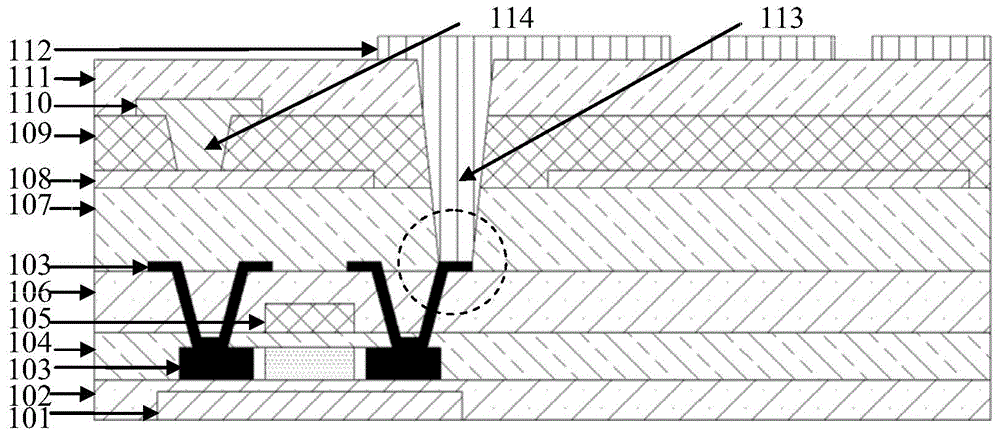
[0028] figure 1 It is a schematic structural diagram of an LTPS array substrate fabricated by the prior art. figure 1 The switching element shown in is a thin film transistor arranged in a top-gate structure. Wherein, 101 is a light-shielding layer, and 102 is a buffer layer, which are respectively used to shield the backlight of the substrate and the influence of defects on the substrate. 10...


PUM


Abstract

The invention discloses a LTPS array substrate and a manufacturing method thereof; the array substrate manufacturing method comprises the following steps: etching an organic film covering a film transistor so as to form a first through hole, and the first through hole exposes a metal layer on which a source electrode or drain electrode of the film transistor are located; forming a protection layer in the first through hole so as to cover the metal layer on which the source electrode or the drain electrode are located; using at least one etching so as to etch a multilayer film formed before a pixel electrode and covering the protection layer, so the pixel electrode makes contact with the protection layer; the method can effectively prevent the source electrode or the drain electrode from being overly etched in a through hole processing step, is simple and fast, and can be promoted by using an existing production line.

Description

technical field [0001] The invention relates to the field of processing and manufacturing of liquid crystal displays, in particular to an LTPS array substrate and a manufacturing method thereof. Background technique [0002] Low Temperature Polysilicon (LTPS) is a liquid crystal display technology widely used in small and medium-sized electronic products such as tablet computers and mobile communication devices. Compared with the traditional amorphous silicon liquid crystal display, the low-temperature polysilicon liquid crystal display has many advantages such as high resolution, fast response speed, large aperture ratio, and high display brightness. At the same time, the low-temperature polysilicon liquid crystal display can also manufacture peripheral driving circuits on the glass substrate, which is beneficial to reduce connection components, save space and production costs, and improve product reliability and stability. [0003] But on the other hand, due to the small ...

Claims


Application Information

Patent Timeline
Patent Type & Authority Applications(China)
IPC IPC(8): H01L21/84H01L27/12H01L27/28
CPCH01L27/1214H01L27/1259H01L21/02697H01L2021/775H10K19/10
Inventor 陈归薛景峰
Owner WUHAN CHINA STAR OPTOELECTRONICS TECH CO LTD
Why Eureka
Try Eureka