Pixel unit, preparation method thereof, array substrate and display device
A technology for pixel units and array substrates, applied in electrical components, semiconductor/solid-state device manufacturing, optics, etc., can solve the problems of limited space size of via holes, difficult to realize, reduce the slope of via holes, etc., and reduce the cracking of conductive materials risk effect
- Summary
- Abstract
- Description
- Claims
- Application Information
AI Technical Summary
Problems solved by technology
Method used
Image
Examples
no. 1 example
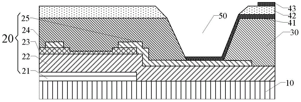
[0039] In this embodiment, a pixel unit is provided. Refer below image 3 The structure of the pixel unit of this embodiment will be described in detail. It should be clarified that the pixel unit defined in this embodiment does not include gate lines and data lines. The pixel unit can be used to form a common array substrate or a dual-gate array substrate after the gate lines and data lines are properly arranged.
[0040] image 3 It is a schematic structural diagram of a pixel unit according to the first embodiment of the present invention. Please refer to image 3 , the pixel unit in this embodiment includes: a thin film transistor 20 , a pixel electrode 41 and a common electrode 43 .
[0041] The thin film transistor 20 is a bottom gate field effect transistor, comprising: a gate 21, a gate insulating layer 22 formed above the gate 21, an active layer 23 formed above the gate insulating layer 22, and an active layer 23 formed on the active layer 23. source 24 and dra...
no. 3 example
[0089] In this embodiment, an array substrate is provided. Figure 5 It is a top view of the array substrate according to the third embodiment of the present invention. For the purpose of clearly describing this embodiment, the passivation layer and the common electrode above the pixel electrodes are omitted.
[0090] Please refer to Figure 5 , the array substrate includes: a glass substrate; gate lines 1 formed on the glass substrate; and data lines 2 formed on the glass substrate and substantially perpendicular to the gate lines 1 . Among them, several pixel regions are defined between the gate line 1 and the data line 2 . Each pixel area includes what is described in Embodiment 1, such as image 3 Pixel units shown.
[0091] In the pixel unit, the gate of the thin film transistor is connected to the gate line, and the source of the thin film transistor is connected to the data line.
[0092] As an array substrate in this embodiment, it may be the following array subst...
no. 5 example
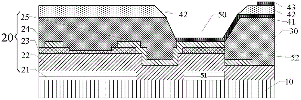
[0097] In this embodiment, an array substrate is provided. The difference between the array substrate and the array substrate of the third embodiment is that it is an array substrate using OLED technology. Specifically, in the pixel unit, the common electrode and the pixel electrode are not separated by a passivation layer, but have an organic light-emitting layer. Under the condition that the common electrode and the pixel electrode provide voltage, the organic light-emitting layer can emit light with preset colors and gray scales. Regarding the content of the via hole, reference may be made to the content of the first embodiment; for the content of the organic light emitting layer, reference may be made to relevant documents in the prior art, and details will not be repeated here.
PUM
 Abstract
Description
Claims
Application Information


