GaN-based LED epitaxial structure having asymmetric super-lattice layer and preparation method for same

A technology of superlattice layer and epitaxial structure, applied in electrical components, circuits, semiconductor devices, etc., can solve the problems of hindering the ability to activate lateral expansion, adverse luminous efficiency, etc., so as to improve the overall luminous efficiency, improve the injection efficiency, and reduce the luminescence. The effect of reducing efficiency

Active Publication Date: 2015-08-26
FOCUS LIGHTINGS SCI & TECH
View PDF5 Cites 6 Cited by
  • Summary
  • Abstract
  • Description
  • Claims
  • Application Information

AI Technical Summary

Problems solved by technology

However, it hinders the activation and lateral expansion of holes, which is not conducive to improving the overall luminous efficiency of LEDs.

Method used


Image

  • GaN-based LED epitaxial structure having asymmetric super-lattice layer and preparation method for same
  • GaN-based LED epitaxial structure having asymmetric super-lattice layer and preparation method for same

Examples


Embodiment Construction

[0033] In order to enable those skilled in the art to better understand the technical solutions in the present invention, the following will clearly and completely describe the technical solutions in the embodiments of the present invention with reference to the accompanying drawings in the embodiments of the present invention. Obviously, the described The embodiments are only a part of the embodiments of the present invention, rather than all the embodiments. Based on the embodiments of the present invention, all other embodiments obtained by those of ordinary skill in the art without creative work shall fall within the protection scope of the present invention.

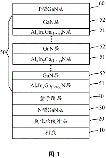
[0034] Participate figure 1 As shown, the present invention discloses a GaN-based LED epitaxial structure with an asymmetric superlattice layer, which sequentially includes:

[0035] The substrate 10, the substrate material is usually a sapphire substrate, but may also be other substrate materials, such as Si, SiC, etc....


PUM


Abstract

The invention discloses a GaN-based LED epitaxial structure having an asymmetric super-lattice layer and a preparation method for the same. The GaN-based LED epitaxial structure comprises a substrate, a nitride buffer layer, an N-type GaN layer, a quantum well layer, the asymmetric super-lattice layer and a P-type GaN layer which are sequentially arranged from bottom to top. The asymmetric super-lattice layer is composed of multiple AlxInyGa(1-x-y)N/GaN super-lattice layer units which are sequentially stacked, the total thickness of an AlxInyGa(1-x-y)N layer and a GaN layer in each different period is the same, the thicknesses of the AlxInyGa(1-x-y)N layers gradually decrease as the number of circles changes, and the thicknesses of the GaN layers increase as the number of circles changes. According to the invention, the asymmetric super-lattice layer reduces the limitation on cavity vertical migration and improves the cavity injection efficiency, the AlxInyGa(1-x-y)N layers whose thicknesses progressively change can gradually assist cavities in expanding laterally in a ladder pattern manner, so that the overall luminescence efficiency of an LED device can be improved.

Description

Technical field [0001] The invention relates to the technical field of semiconductor light-emitting devices, in particular to a GaN-based LED epitaxial structure with an asymmetric superlattice layer and a preparation method thereof. Background technique [0002] Light-Emitting Diode (LED) is a semiconductor electronic component that can emit light. This kind of electronic components appeared as early as 1962. In the early days, it could only emit low-luminosity red light. Later, other monochromatic versions were developed. The light that can be emitted today has spread to visible light, infrared and ultraviolet light, and the luminosity has also increased to a considerable extent. 的光度. The use has also been used as indicator lights, display panels, etc. from the beginning; with the continuous advancement of technology, light-emitting diodes have been widely used in display, television lighting decoration and lighting. [0003] Although high-brightness LED chips have been commerci...

Claims


Application Information

Patent Timeline
Patent Type & Authority Applications(China)
IPC IPC(8): H01L33/06H01L33/00
CPCH01L33/0066H01L33/06
Inventor 冯猛刘恒山蔡睿彦陈立人
Owner FOCUS LIGHTINGS SCI & TECH
Why Eureka
Try Eureka