
Curved-surface LED display backboard stamping die machining method

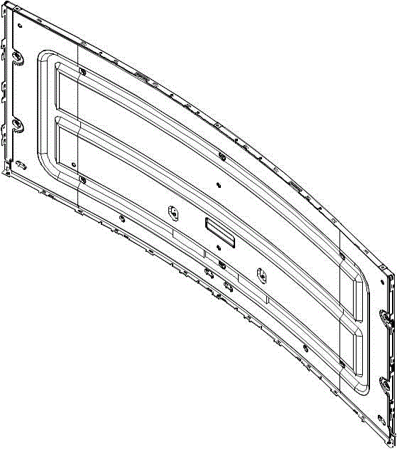
A liquid crystal display, curved surface technology, applied in metal processing equipment, forming tools, manufacturing tools and other directions, can solve the problems of material waste, waste of manpower, large space, etc., to achieve simple cutting and blanking engineering, stable and reliable forming, forming simple structure

Inactive Publication Date: 2015-09-09
JIANGSU FANRUN ELECTRONICS
View PDF0 Cites 14 Cited by
  • Summary
  • Abstract
  • Description
  • Claims
  • Application Information

AI Technical Summary

Problems solved by technology

[0006] The technical defect of the above-mentioned method 1 scheme is that the processes such as positioning holes, protrusions, depressions, chamfers, hooks, and buds are completed first on the plane reference, and after the curved surface is formed, the relative positions of these process shapes occur. Changes, large deviations in size
Unstable product quality increases assembly difficulty
[0007] In method 2, although the curved surface is completed first and then other processes are completed, it overcomes the problem of unstable assembly dimensions in method 1, but the box-like stretching of the curved surface itself has new defects:
[0008] 1. The material utilization rate is low, the upper and lower box-shaped structures of the stretched body are auxiliary parts, and the subsequent engineering needs to be cut off, resulting in waste of materials;
[0009] 2. When stretching the box body for shape punching, the punching waste is composed of the side and extension of the box body. The waste material is in a special-shaped three-dimensional shape and takes up a lot of space. If more than 4 pieces of waste material accumulate, it may cause blockage, so the production must be carried out manually. processing, wasting manpower

Method used


Image

  • Curved-surface LED display backboard stamping die machining method
  • Curved-surface LED display backboard stamping die machining method
  • Curved-surface LED display backboard stamping die machining method

Examples


Embodiment Construction

[0026] Below in conjunction with accompanying drawing, the mode of the present invention is further elaborated:

[0027] According to the invention scheme, 6 sets of molds made according to the new scheme are respectively installed on 6 stamping machines, and the installation and debugging are in place.

[0028] The general division of labor is as follows:

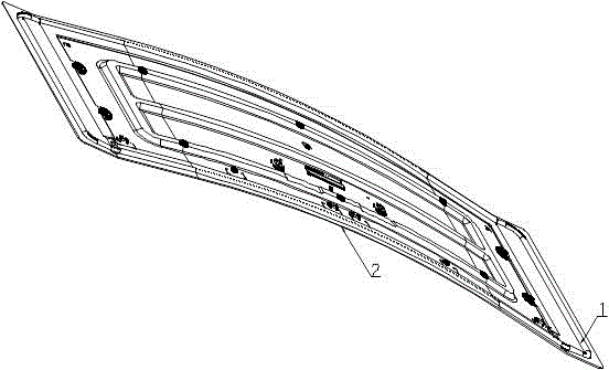
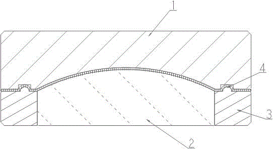
[0029] The sheet material enters the No. 1 punching machine, the working surface is a curved surface and the pressing plate with ribs moves down to press the blank on the die with the same working surface as a curved surface, and then the punch goes down into the die to form the blank It is a surface sheet, and the convex hull on the surface is also stretched together.

[0030] The semi-finished product in the No. 1 punching machine is taken out by the mechanical arm and transferred to the No. 2 punching machine. The shape of the product is cut, the convex hull is shaped on the curved surface, and the hook is formed.

[...


PUM


Abstract

The invention relates to a curved-surface LED display backboard stamping die machining method. The method is characterized in that used raw materials are sheets, the sheets are formed into curved-surface sheet bodies on first project curved surfaces, and other subsequent processes such as trimming, convex hull shaping, clamp hook forming, hole stamping, engraving, burr pressing, little bending, engraving, sprouting and complete-cycle bending are all finished on the formed curved-surface sheet bodies. During curved-surface forming, a male die, a female die and a pressure plate are provided, the working surface is a curved surface, pressing ribs are arranged on the die pressure plate, stretching and curved-surface stabilization are facilitated, and accordingly production efficiency is increased, and waste is reduced.

Description

technical field [0001] The invention relates to a method for processing a stamping die for a backplane of an important structural component (BOT CHASSIS) of a curved surface LED display. Background technique [0002] (OLED BOT CHASSIS) curved backplane is an important structural component used to install curved liquid crystal panels and circuit boards. The structure of the curved backplane is similar to that of the flat backplane. There are forming surfaces with bent edges on all sides. There are many positioning holes, protrusions, depressions, chamfers, undulations of various shapes, hooks, sprouts, etc. structure, the difference is that all the process structures of the curved backplane are completed on the curved surface, which is more difficult to produce. [0003] Existing mold production methods: [0004] Method 1: Before the final bending forming process, it is produced according to the general flat back panel method, and the curved surface process is completed at ...

Claims


Application Information

Patent Timeline
IPC IPC(8): B21D37/10
CPCB21D37/10
Inventor 关超朴日模
Owner JIANGSU FANRUN ELECTRONICS
Learn More