
Method and apparatus for preparing black silica by adopting lattice scanning

A black silicon and lattice technology, applied in the field of semiconductor optoelectronic material preparation, can solve the problems of long time consumption and slow processing speed of black silicon, and achieve the effects of avoiding dispersion, ensuring beam quality and improving preparation efficiency.

Inactive Publication Date: 2015-09-09
BEIJING CHANGCHENG INST OF METROLOGY & MEASUREMENT AVIATION IND CORP OF CHINA
View PDF6 Cites 4 Cited by
  • Summary
  • Abstract
  • Description
  • Claims
  • Application Information

AI Technical Summary

Problems solved by technology

[0016] The purpose of the present invention is to solve the problem that the traditional point-by-point scanning method of preparing black silicon has a slow processing speed and takes a long time when preparing large-area black silicon, and provides a method and device for preparing black silicon by dot-matrix scanning

Method used


Image

  • Method and apparatus for preparing black silica by adopting lattice scanning
  • Method and apparatus for preparing black silica by adopting lattice scanning
  • Method and apparatus for preparing black silica by adopting lattice scanning

Examples


Embodiment Construction

[0032] The present invention will be described in detail below in conjunction with the accompanying drawings and embodiments.

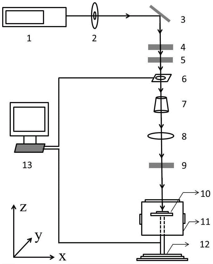
[0033] Such as figure 2 As shown, a device for preparing black silicon by dot matrix scanning includes a laser 1, an aperture 2, a mirror 3, a half-wave plate 4, a polarizer 5, a shutter 6, a beam expander 7, a focusing lens 8, and a Damman grating 9. Sample holder 10, sample chamber 11, three-dimensional translation stage 12, computer 13. The computer 13 controls the opening and closing of the shutter 6 and the movement of the three-dimensional translation platform 12 respectively through the shutter controller and the three-dimensional translation platform controller.

[0034] A kind of dot-matrix scanning prepares the method for black silicon, comprises the following steps:

[0035] Step 1: Place the silicon wafer on the sample holder 10, evacuate the sample chamber 11, and fill the sample chamber 11 with a certain pressure of SF after reaching ...


PUM

PropertyMeasurementUnit
laser poweraaaaaaaaaa

Abstract

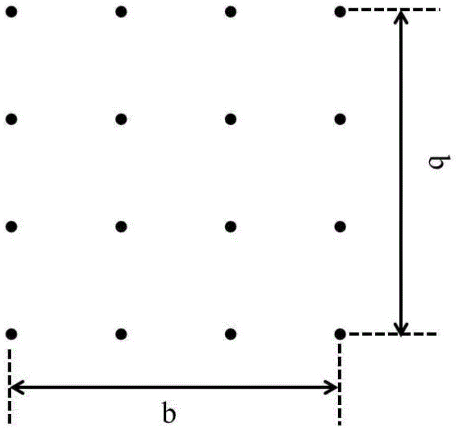
The invention relates to a method and apparatus for preparing black silica by adopting lattice scanning. The method includes the following steps that: 1, a silicon wafer is arranged in a doped material-containing sample chamber; 2, a single laser beam of a pulse laser passes through a diaphragm, a reflector, a half wave plate, a polarizer, a shutter, a beam expanding mirror, a focusing lens, a Dammann grating and the like, so that lattice laser can be obtained; 3, the lattice laser irradiates on the surface of the silicon wafer, and a computer controls the opening and closing of the shutter and the movement of a three-dimensional translational platform, and therefore, lattice scanning can be realized, and a black silica material of which the surface is of a micro pointed cone structure can be obtained. According to the method and apparatus of the invention, the Dammam grating is adopted, and the single beam laser can be converted into two-dimensional and equal-light intensity array beams; when the Dammam grating splits the laser beam, the influence of chromatic dispersion in the light splitting process of an ordinary semi-transmittance and semi-reflection mirror can be avoided, and the quality of the split light beams can be ensured; and point-by-point scanning adopted for preparing the black silica is converted into lattice scanning, and therefore, the preparation efficiency of the black silica can be greatly improved.

Description

technical field [0001] The invention relates to the field of semiconductor optoelectronic material preparation, in particular to a method and device for preparing black silicon by lattice scanning. Background technique [0002] Black silicon refers to a material with a periodic microstructure on the surface obtained by etching single crystal silicon by physical or chemical methods. Black silicon has a high absorption rate for visible light and near-infrared light, and the absorption rate can reach 90% in the range of 0.25 μm to 2.5 μm. In 2005, the black silicon photodiode detector prepared by the research team of Professor Eric Mazur irradiated n(111) silicon substrate with femtosecond laser, under the reverse bias of 0.5V at room temperature, the photoelectric responsivity at 1000nm was 120A / W, two orders of magnitude higher than commercial silicon detectors (Opt. Lett., 2005, 30(14), 1773). Due to its excellent properties, black silicon materials have great potential i...

Claims


Application Information

Patent Timeline
Patent Type & Authority Applications(China)
IPC IPC(8): H01L21/02B23K26/00
CPCH01L21/0203B23K26/3584
Inventor 李维武腾飞王宇张力李文斌梁志国
Owner BEIJING CHANGCHENG INST OF METROLOGY & MEASUREMENT AVIATION IND CORP OF CHINA
Learn More