Eureka AIR delivers breakthrough ideas for toughest innovation challenges, trusted by R&D personnel around the world.

Self-aligned double patterning method and fin field effect transistor manufacturing method

A double patterning and fin field effect technology, which is applied in the production of fin field effect transistors and the field of self-alignment double patterning, can solve the problem of shape asymmetry, damage the electrical performance of semiconductor devices, and affect the pattern to be etched 21 Shape and other problems, to achieve the effect of improving electrical performance

Active Publication Date: 2015-09-09
SEMICON MFG INT (SHANGHAI) CORP
View PDF6 Cites 21 Cited by
  • Summary
  • Abstract
  • Description
  • Claims
  • Application Information

AI Technical Summary

Problems solved by technology

[0009] However, after the sidewall 51 is formed by the above process, the cross section of the sidewall 51 is tapered and its shape is asymmetric, so that the material layer 20 to be etched is etched using the sidewall 51 as a mask. , it will affect the morphology of the final pattern to be etched 21, and eventually damage the electrical performance of the subsequently formed semiconductor device

Method used


Image

  • Self-aligned double patterning method and fin field effect transistor manufacturing method
  • Self-aligned double patterning method and fin field effect transistor manufacturing method
  • Self-aligned double patterning method and fin field effect transistor manufacturing method

Examples


Embodiment Construction

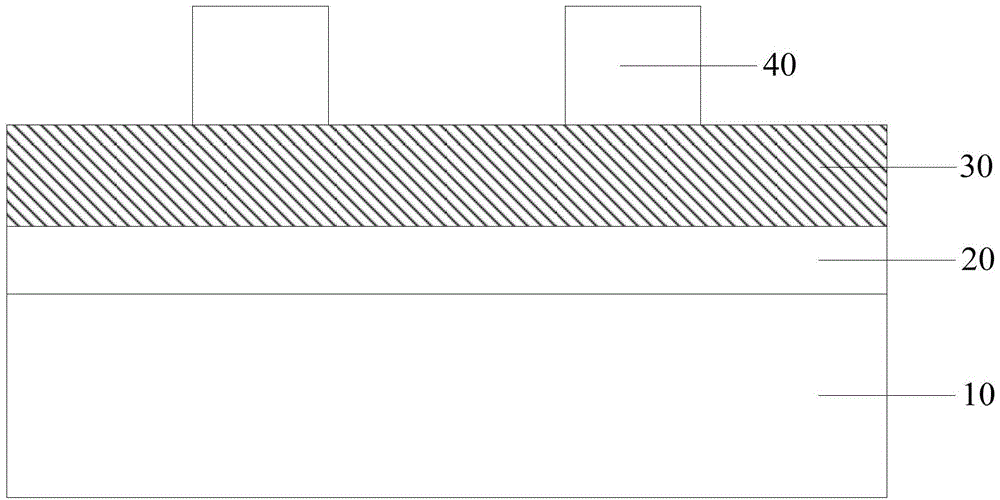
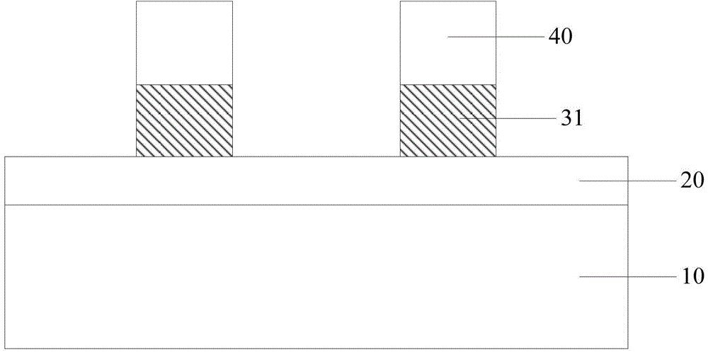
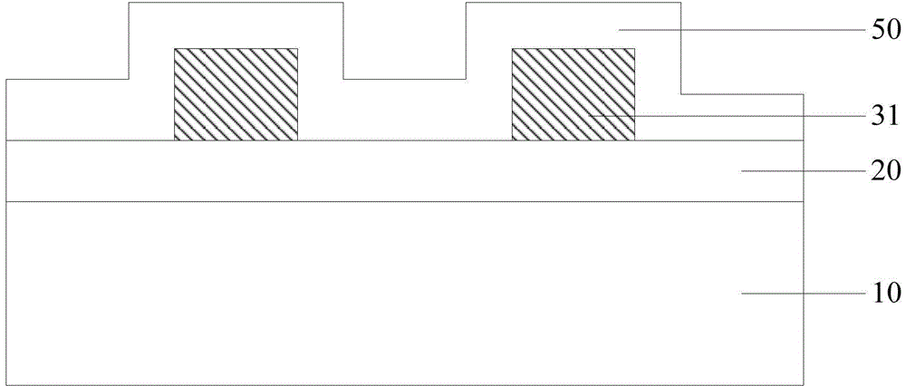
[0029] As described in the background art section, after the prior art SADP technology is used to etch the material layer to be etched, the etching mask obtained by the sidewall process (ie, sidewall) has a pyramidal and asymmetrical appearance. Specifically, the sidewall of the sidewall on the side close to the sacrificial layer pattern is perpendicular to the surface of the semiconductor substrate, and the shape of the sidewall on the side far from the sacrificial layer pattern is arc, so that the sidewalls on both sides of the sidewall The profile shape is different. Therefore, when the material layer to be etched is etched using such sidewall spacers as a mask, the topography of the sidewalls of the material layer to be etched corresponding to both sides of the sidewall spacers are different, which will affect the electrical performance of the semiconductor device to be subsequently formed.

[0030] In view of the above-mentioned problems, the present invention provides a sel...


PUM

PropertyMeasurementUnit
Thicknessaaaaaaaaaa
Thicknessaaaaaaaaaa

Abstract

Provided are a self-aligned double patterning method and a fin field effect transistor manufacturing method. The self-aligned double patterning method comprises: providing a material layer to be etched; successively forming a first sacrificial layer and a photoresist pattern on the material layer to be etched; etching the first sacrificial layer by using the photoresist pattern as a mask in order to form a first sacrificial layer pattern; removing the photoresist pattern and forming a mask material layer covering the first sacrificial layer pattern on the material layer to be etched; forming a second sacrificial layer on the mask material layer; removing the second sacrificial layer and the mask material layer on the first sacrificial layer pattern; removing the rest second sacrificial layer; etching the rest mask material layer until the material layer to be etched is exposed; removing the first sacrificial layer pattern; and etching the material layer to be etched by using the rest mask material layer as a mask. The fin field effect transistor manufacturing method comprises the above self-aligned double patterning method. A symmetric mask with a rectangular cross section can be formed by using the methods.

Description

Technical field [0001] The invention relates to the technical field of semiconductor manufacturing, in particular to a self-aligned dual patterning method and a method for manufacturing a fin field effect transistor. Background technique [0002] In the field of semiconductor manufacturing, photoresist materials are used to transfer mask patterns to one or more layers of materials, for example, to transfer mask patterns to metal layers, dielectric layers or semiconductor substrates. However, as the feature size of the semiconductor process continues to shrink, it becomes more and more difficult to form a mask pattern with a small feature size in the material layer using a photolithography process. [0003] In order to improve the integration of semiconductor devices, the industry has proposed a variety of double patterning processes. Among them, the self-aligned double patterning (SADP) process is one of them. Refer to Figure 1 to Figure 5 Shown. [0004] reference figure 1 As show...

Claims


Application Information

Patent Timeline
IPC IPC(8): H01L21/033H01L21/336
CPCH01L21/033H01L29/66795
Inventor 何永根
Owner SEMICON MFG INT (SHANGHAI) CORP
Why Eureka
Eureka Blog
Learn More