Orifice burr removing method and apparatus

A burr and orifice technology, applied in the field of circuit board production, to improve processing efficiency and increase cutting volume

Active Publication Date: 2015-09-16
JIANGMEN SUNTAK CIRCUIT TECH
View PDF4 Cites 16 Cited by
  • Summary
  • Abstract
  • Description
  • Claims
  • Application Information

AI Technical Summary

Problems solved by technology

[0003] The present invention aims at the problem that it is difficult to completely remove the burr at the hole in the existing method for making metallized holes, which leads to the problem of quality hidden d...

Method used


Image

  • Orifice burr removing method and apparatus
  • Orifice burr removing method and apparatus

Examples


Embodiment

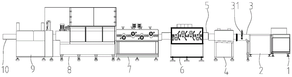
[0024] refer to Figure 1-2 , this embodiment provides a method for removing burrs from an orifice, and a device for removing burrs from an orifice using this method.

[0025] Firstly, according to the circuit board production process in the prior art, the base material is cut to obtain a base plate for preparing each inner layer board. After the conventional pretreatment of the substrate, the inner layer circuit pattern is made on the substrate through the steps of applying wet film on the substrate, exposing, developing, etching, and stripping the film (negative film process), thereby making each inner layer board. Inspect and evaluate the quality of each inner layer board through inner layer AOI.

[0026] Then, the inner layer board is browned by using the existing browning process of the inner layer board before lamination, so that a layer of brown oxide is formed on the inner layer board, and the surface of the inner layer board is roughened. Then, according to the desi...


PUM

PropertyMeasurementUnit
Widthaaaaaaaaaa

Abstract

The invention belongs to the circuit board production technical field and relates to an orifice burr removing method and apparatus. The method of the invention mainly comprises the following steps that: an abrasive band grinding machine and a precision grinding machine are additionally adopted; the surface of a multilayer board is ground through the abrasive band grinding machine; the surface of the multilayer board is ground through the precision grinding machine; and then, the surface of the multilayer board is ground through a rough grinding machine. With the method of the invention adopted, the cutting output of a board grinding section can be increased, so that orifice burrs can be completely cut off assuredly, and therefore, problems such as hidden troubles in quality which are caused by inexistence of copper in orifices or cooper wire formation in the orifices which are further caused by a situation that a dry film is pierced in a following production process can be solved; and the abrasive band grinding machine and the precision grinding machine are in line connection with the rough grinding machine, so that the processing efficiency of the orifice burrs can be improved.

Description

technical field [0001] The invention relates to the technical field of circuit board production, in particular to a method and device for removing burrs from orifices. Background technique [0002] PCB (Printed Circuit Board) is one of the important components of the electronics industry, a support for electronic components, and a carrier for electrical connections. With the continuous update of electronic product application technology and the improvement of functions, the design of PCB is becoming more and more precise, dense and high-performance. For multi-layer PCBs, the circuit conduction between layers is realized by drilling and metallizing the holes. The existing process is generally: making multi-layer boards in the previous process → drilling → coarse grinding machine grinding → copper sinking → Whole board electroplating → post process. However, after drilling holes on multi-layer boards, burrs are easy to appear at the holes, especially for multi-layer boards w...

Claims


Application Information

Patent Timeline
IPC IPC(8): H05K3/00H05K3/46
CPCH05K3/0055H05K3/46H05K2203/025
Inventor 张义兵徐文中张柳潘捷
Owner JIANGMEN SUNTAK CIRCUIT TECH
Why Eureka
Try Eureka