Semiconductor structure and formation method thereof

A semiconductor and patterning technology, applied in semiconductor devices, semiconductor/solid-state device manufacturing, electrical components, etc., can solve problems such as the inability to control the threshold voltage of fin field effect transistors, and achieve improved short-channel effects and increased channel lengths , the effect of high channel length

Active Publication Date: 2015-09-30
SEMICON MFG INT (SHANGHAI) CORP
View PDF3 Cites 0 Cited by
  • Summary
  • Abstract
  • Description
  • Claims
  • Application Information

AI Technical Summary

Problems solved by technology

However, it is difficult to bias the channel region of MGFETs, for example, transistors with surrounding gate structures (refer to figure 1 ), the gate structure 20 completely surrounds the channel region 10 in the center, so it is difficult to apply a bias voltage to the channel region 10; for the fin field effect transistor (please refer to figure 2 ), the channel region is located on the surface of the fin portion 40, and the distance from the substrate 30 is relatively large, so applying a bias voltage to the substrate 30 has little effect on the channel region, and it is impossible to realize the fin by applying a bias voltage to the substrate 30 Threshold voltage control of type field effect transistor

Method used


Image

  • Semiconductor structure and formation method thereof
  • Semiconductor structure and formation method thereof
  • Semiconductor structure and formation method thereof

Examples


Embodiment Construction

[0034] As mentioned in the background, the multi-gate transistor formed in the prior art cannot adjust the threshold voltage of the transistor by applying a bias voltage.

[0035] In the embodiment of the present invention, while forming a transistor with a multi-gate structure, a back gate is formed on the other side of the channel layer, so that a bias voltage can be applied to the channel layer through the back gate, thereby adjusting the threshold voltage of the transistor .

[0036] In order to make the above objects, features and advantages of the present invention more comprehensible, specific embodiments of the present invention will be described in detail below in conjunction with the accompanying drawings.

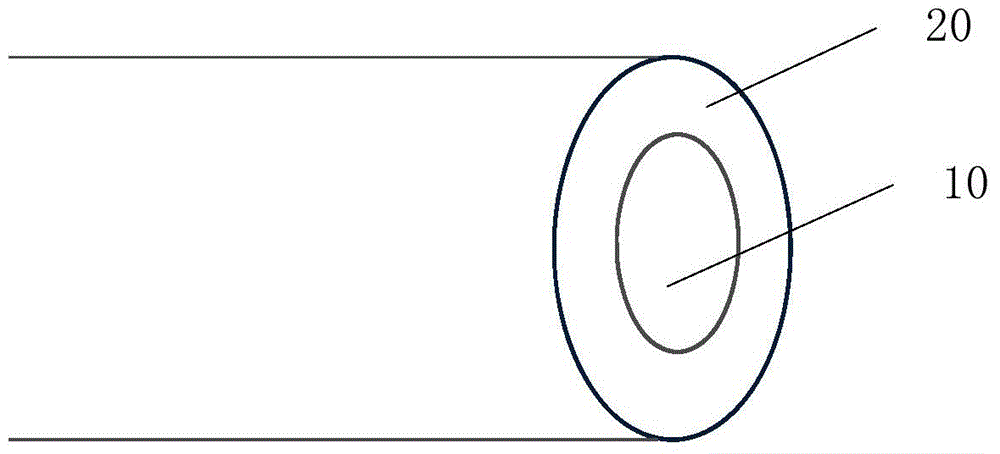
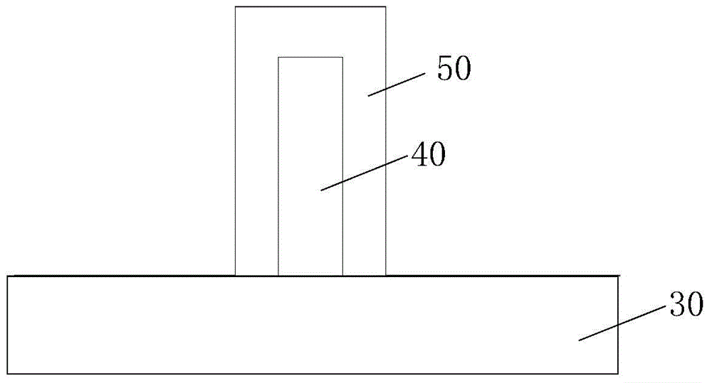
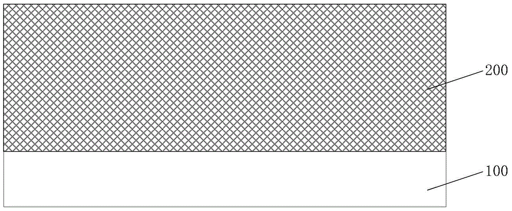
[0037] Please refer to image 3 1. A substrate 100 is provided, and a gate material layer 200 is formed on the surface of the substrate 100 .

[0038] The material of the substrate 100 includes semiconductor materials such as silicon, germanium, silicon germani...


PUM

PropertyMeasurementUnit
Thicknessaaaaaaaaaa

Abstract

The invention provides a semiconductor structure and a formation method thereof. The formation method of the semiconductor structure includes providing a substrate; forming a projecting grid on the surface of the substrate; forming gate medium layers on the surfaces of the side walls of the grid; forming a channel layer on the surface of the grid medium layer; forming a medium layer on the surface of the substrate; forming a first through hole in the medium layer on each side of the grid, wherein a part of the medium layer is arranged between the first through hole and the channel layer; and forming back grids in the first through holes. The semiconductor structure formed by adopting the above method has a comparatively large channel length and can adjust the threshold voltage of a transistor by exerting voltage on the channel layer through the back grids.

Description

technical field [0001] The invention relates to the technical field of semiconductors, in particular to a semiconductor structure and a forming method thereof. Background technique [0002] With the continuous development of semiconductor process technology, the process node is gradually reduced, and the gate-last (gate-last) process has been widely used to obtain an ideal threshold voltage and improve device performance. However, when the feature size of the device is further reduced, even if the gate-last process is adopted, the structure of the conventional MOS field effect transistor can no longer meet the requirements of device performance. A larger channel length can effectively improve the short-channel effect of the transistor, and thus has received extensive attention. [0003] The threshold voltage of transistors can be adjusted by implanting dopant ions into the channel region, but as the size of transistors continues to shrink, it becomes more and more difficult...

Claims


Application Information

Patent Timeline
IPC IPC(8): H01L21/336H01L21/28H01L29/78H01L29/10H01L29/49
Inventor 三重野文健
Owner SEMICON MFG INT (SHANGHAI) CORP
Why Eureka
Try Eureka