Method for forming selective metal lines on plastic surface and plastic part

A metal circuit, selective technology, applied in the direction of metal material coating process, printed circuit, electrical components, etc., can solve the problems of high cost, high cost and high cost of bearing materials, achieve good selective plating, and reduce material requirements , the effect of expanding the scope of application

Active Publication Date: 2019-07-12
苏州同拓光电科技有限公司
View PDF6 Cites 0 Cited by
  • Summary
  • Abstract
  • Description
  • Claims
  • Application Information

AI Technical Summary

Problems solved by technology

However, the disclosed method is costly
Firstly, the non-conductive metal compound incorporated in the non-conductive carrier material for the manufacture of the conductor track structure is highly thermally stable, stable and insoluble in aqueous acidic or alkaline metallization electrolytes, non-conductive Based on higher-order oxides of spinel or simple d-metal oxides or mixtures thereof similar in structure to spinel, it can be seen that the performance and structure requirements of the non-conductive metal compound are relatively high, and the price is expensive; secondly, it can The cost of carrying materials mixed with the above-mentioned non-conductive metal compounds is relatively high, which also causes certain restrictions.
[0004] It can be seen that the LDS process requires special materials, and the metal compound necessary for the LDS process is added to the material. Due to the large proportion of the addition, the modified material has no effect on the thermal stability and compatibility of the metal compound and the plastic substrate. , plasticizing stability, electrical performance stability and other aspects have a greater impact, which increases the cost and limits the scope of application of the material

Method used


Image

  • Method for forming selective metal lines on plastic surface and plastic part
  • Method for forming selective metal lines on plastic surface and plastic part
  • Method for forming selective metal lines on plastic surface and plastic part

Examples


Embodiment Construction

[0033] In the following description, many technical details are proposed in order to enable readers to better understand the application. However, those skilled in the art can understand that without these technical details and various changes and modifications based on the following implementation modes, the technical solution claimed in each claim of the present application can be realized.

[0034] In order to make the purpose, technical solution and advantages of the present invention clearer, the following will further describe the implementation of the present invention in detail in conjunction with the accompanying drawings.

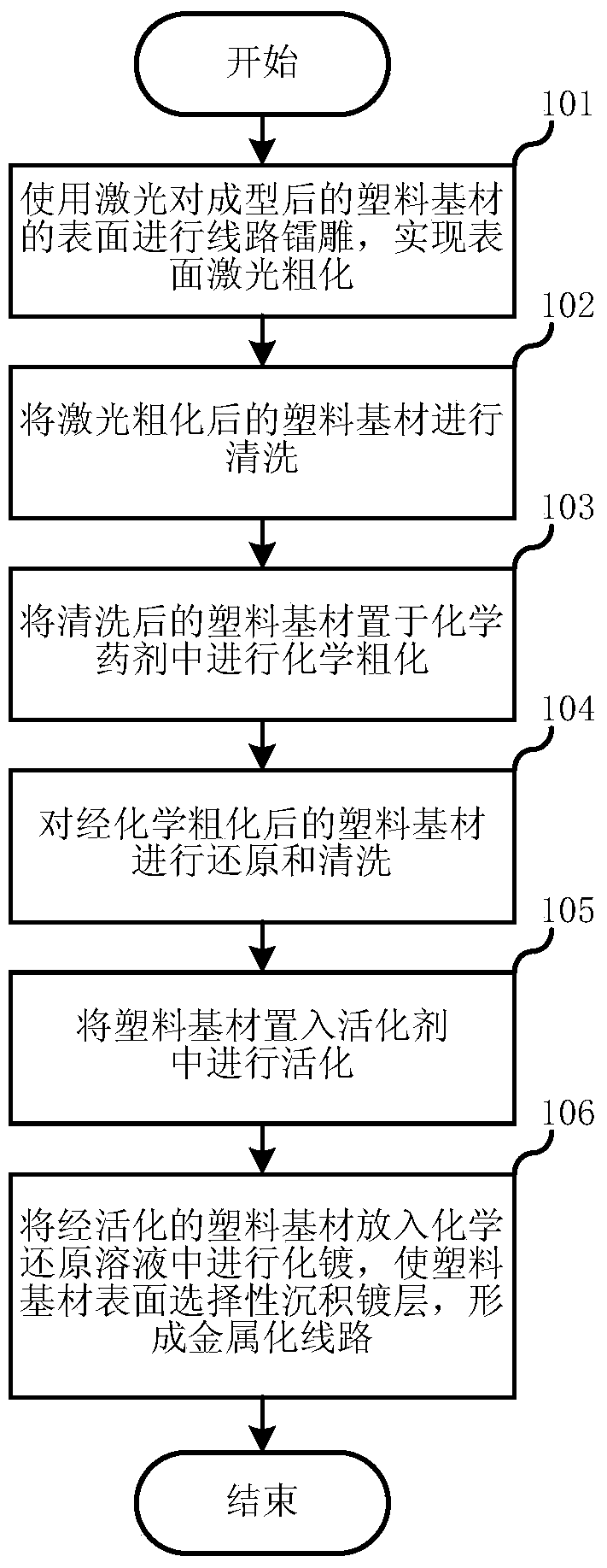
[0035] The first embodiment of the present invention relates to a method of forming selective metal lines on a plastic surface, figure 1 is a schematic flow chart of the method for forming selective metal circuits on plastic surfaces.

[0036] Specifically, as figure 1 As shown, the method for forming a selective metal circuit on a plastic surfa...


PUM


Abstract

A method of forming a selective metal circuit on a plastic surface, comprising the following steps: conducting laser etching on a shaped plastic substrate surface with laser to realize laser roughening; cleaning the plastic substrate; placing the plastic substrate into a chemical agent for chemical roughening; conducting reduction and cleaning after chemical roughening; placing the plastic substrate into an activator for activation; and conducting chemical plating to selectively deposit plating to form a metalized circuit. Also provided is a plastic component having the metal circuit on the surface, the metal circuit being formed on a plastic component surface by employing the above method.

Description

technical field [0001] The present invention relates to the manufacture of conductor structures, and more particularly to methods and plastic components for forming selective metal circuits on plastic surfaces. Background technique [0002] Laser Direct Structuring (LDS for short) technology is one of the current methods to realize three-dimensional circuits. Its process is to use special materials to make structural parts (the material can be activated by laser to achieve selective plating) , Mark the required graphics on the surface of the workpiece by laser, and then electroplate a metal layer to form a circuit. [0003] Chinese Patent No. 02812609 describes a conductor track structure and its manufacturing method. The conductor track structure consists of a metal core and a metallization layer subsequently applied to the metal core. The conductor track structure is located on a non-conductive carrier material into which a non-conductive metal compound has been doped. ...

Claims


Application Information

Patent Timeline
Patent Type & Authority Patents(China)
IPC IPC(8): C23C18/22C23C18/30C23C18/38
CPCC23C18/22H05K3/18
Inventor 王咏
Owner 苏州同拓光电科技有限公司
Why Eureka
Try Eureka