Positioning method for pattern-free silicon chip measurement

A positioning method and a pattern-free technology, which is applied in the direction of measuring devices, semiconductor/solid-state device testing/measurement, and optical devices, etc., can solve the problems of excessive beam measurement position deviation and measurement repeatability cannot be guaranteed, so as to improve the measurement Effect of repeatability, good measurement accuracy

Active Publication Date: 2015-10-14
RAINTREE SCI INSTR SHANGHAI
View PDF8 Cites 4 Cited by
  • Summary
  • Abstract
  • Description
  • Claims
  • Application Information

AI Technical Summary

Problems solved by technology

However, the silicon wafer translation and rotation errors generated during the process are not considered, so it will inevitably lead to excessive

Method used


Image

  • Positioning method for pattern-free silicon chip measurement
  • Positioning method for pattern-free silicon chip measurement
  • Positioning method for pattern-free silicon chip measurement

Examples


Example Embodiment

[0026] In the following detailed description of the preferred embodiments, reference will be made to the attached drawings constituting a part of the present invention. The attached drawings illustrate specific embodiments capable of implementing the present invention by way of example. The illustrated embodiments are not intended to be exhaustive of all embodiments according to the present invention. It can be understood that without departing from the scope of the present invention, other embodiments may be used, and structural or logical modifications may also be made. Therefore, the following detailed description is not restrictive, and the scope of the present invention is defined by the appended claims.

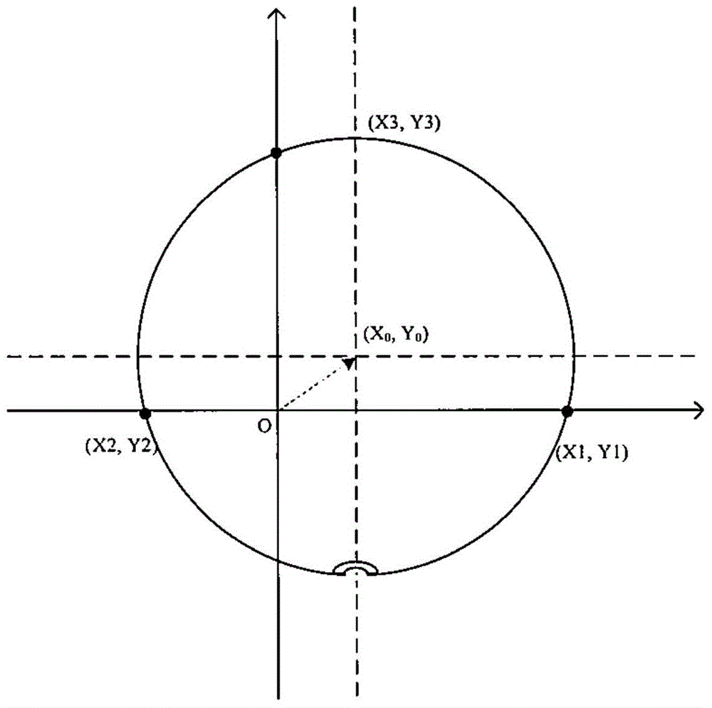
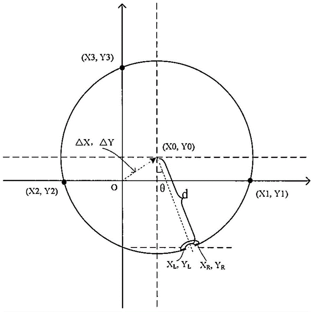
[0027] When measuring silicon wafers, the following two factors cause the problem of low test repeatability during the wafer loading process:

[0028] 1. The translation of the wafer on the wafer, that is, the coordinate value of the center of the wafer on the wafer in the...


PUM


Abstract

The invention discloses a positioning method for pattern-free silicon chip measurement. The method comprises the following steps: A, determining at least three reference points of a silicon chip, obtaining coordinates of the corresponding reference points, and according to the at least three reference points, determining the coordinates of the circle center of the silicon chip and the length of a radius; and B, according to the positioning structure of the silicon chip and the circle center and the radius of the silicon chip, determining a rotation angle of the silicon chip. According to the invention, when a system measures the silicon chip, the measuring precision is good, and the measurement repeatability of the system is improved.

Description

technical field [0001] The invention relates to the field of semiconductor manufacturing equipment, especially a method capable of precisely positioning silicon wafers. Background technique [0002] Ellipsopolarization technology is widely used in the semiconductor production industry. With its non-destructive and high-speed characteristics, it has become the main technology for the measurement of silicon wafer surface material characteristics and optical critical dimensions. [0003] With the development of semiconductor technology, the critical dimension of integrated components has progressed from 1μm to 22nm, and the corresponding requirements for the accuracy and repeatability of ellipsometry have been reached order of magnitude. For unpatterned silicon wafers, the non-uniformity of the thickness of its surface film is far more than order of magnitude. Therefore, even if there is a slight difference in the positioning position of the measuring beam on the wafer sur...

Claims


Application Information

Patent Timeline
IPC IPC(8): H01L21/68H01L21/66G01B11/03G01B11/26
Inventor 周坚黄建华杨江涛王勇
Owner RAINTREE SCI INSTR SHANGHAI
Why Eureka
Try Eureka