Thin-film transistor, array substrate, preparation method thereof, and display device

A technology of thin film transistors and array substrates, applied in the direction of transistors, semiconductor/solid-state device manufacturing, semiconductor devices, etc., can solve the problems of TFT devices that are difficult to turn off, high free carrier concentration, poor stability, etc.

Active Publication Date: 2015-10-14
BOE TECH GRP CO LTD +1
View PDF4 Cites 9 Cited by
  • Summary
  • Abstract
  • Description
  • Claims
  • Application Information

AI Technical Summary

Problems solved by technology

But the mobility of IGZO is still not high enough, about 10cm 2 /V·s around
The mobility of IZO is higher than that of IGZO, but it has more oxygen vacancies and a higher concentration of free carriers, which makes it difficult to turn off TFT devices and has poor stability.
[0004] Generally, oxygen vacancies can be reduced by treating the metal oxide surface with oxyge

Method used


Image

  • Thin-film transistor, array substrate, preparation method thereof, and display device
  • Thin-film transistor, array substrate, preparation method thereof, and display device
  • Thin-film transistor, array substrate, preparation method thereof, and display device

Examples


preparation example Construction

[0043] The preparation method of the embodiment of the present invention has the characteristics of being able to control the concentration of oxygen vacancies and free carriers of the metal oxide, good stability, simple preparation process, and low cost.

[0044] For example, in this method, as figure 2 As shown, the electrochemical oxidation treatment of the metal oxide film includes the following steps.

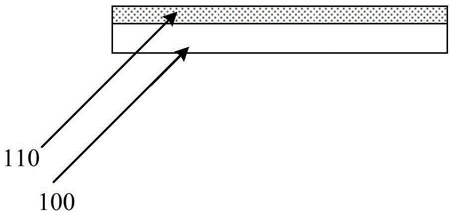
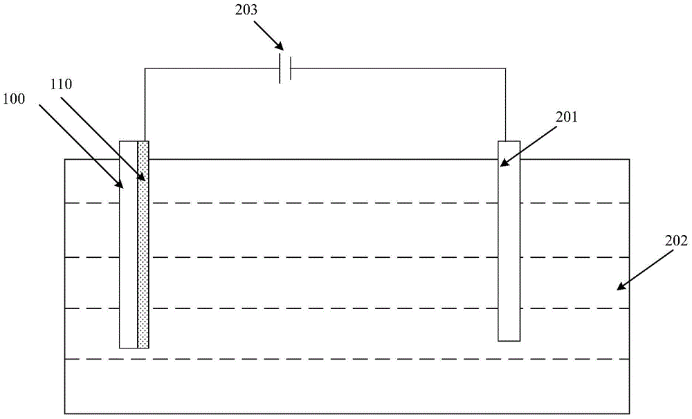
[0045] With the metal oxide film 110 as the anode, the cathode 201 and the substrate 100 formed with the metal oxide film 110 are placed in the electrolytic solution (electrolyte) 202, the metal oxide film 110 and the cathode 201 are respectively connected to the positive pole and the negative pole of the power supply 203 Connected, energized for electrochemical oxidation treatment.

[0046] During the electrochemical oxidation process, the cations of the oxygen vacancies in the metal oxide film will combine with the electrolyzed oxygen, thereby reducing the oxygen vacan...

Embodiment 1

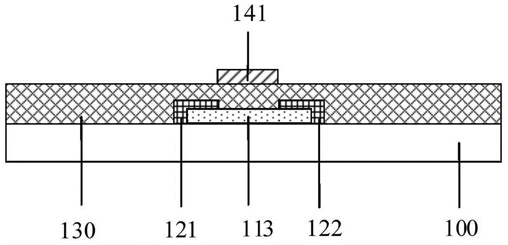
[0061] A kind of metal oxide thin film transistor, its structure is as image 3 As shown, it includes a substrate 100 , an active layer 113 , a source 121 , a drain 122 , a gate insulating layer 130 and a gate 141 . The metal oxide thin film transistor has a top-gate structure. The material of the active layer 113 can be, for example, indium zinc oxide.

[0062] Such as figure 2 As shown in FIG. 4 , the manufacturing method of the metal oxide thin film transistor includes the following steps.

[0063] (1) Form a metal oxide thin film 110 on the substrate 100, such as Figure 4a shown. The metal oxide is, for example, indium zinc oxide.

[0064] (2) Performing electrochemical oxidation treatment on the metal oxide thin film 110 , for example, includes the following steps.

[0065] With the metal oxide film 110 as the anode, the cathode 201 and the substrate 100 formed with the metal oxide film 110 are placed in the electrolyte solution 202, the metal oxide film and the c...

Embodiment 2

[0083] A kind of metal oxide thin film transistor, its structure is as Image 6 As shown, it includes a substrate 100 , an active layer 113 , a source 121 , a drain 122 , a gate insulating layer 130 and a gate 141 . The metal oxide thin film transistor has a bottom gate structure. The material of the active layer 113 is, for example, indium zinc oxide.

[0084] Such as figure 2 As shown in FIG. 7 , the manufacturing method of the metal oxide thin film transistor includes the following steps.

[0085] (1) Form a conductive film 140 on the substrate 100, such as Figure 7a shown, and pattern it to form a gate 141, such as Figure 7b shown.

[0086] For example, a Mo / Al / Mo laminated metal layer can be formed by sputtering, for example, with a thickness of 25nm / 100nm / 25nm respectively, and the gate 141 can be patterned by photolithography.

[0087] (2) forming an insulating film as the gate insulating layer 130, such as Figure 7c shown.

[0088] For example, SiNx and SiO...


PUM

PropertyMeasurementUnit
Thicknessaaaaaaaaaa
Thicknessaaaaaaaaaa
Total thicknessaaaaaaaaaa

Abstract

The invention provides a thin-film transistor, an array substrate, a preparation method thereof, and a display device. The preparation method of the thin-film transistor comprises forming a gate electrode, a gate electrode insulating layer, an active layer, a source electrode and a drain electrode of the thin-film transistor, wherein the active layer is prepared by a metal oxide. Furthermore an electrochemical oxidation treatment is performed on a metal oxide film in the preparing process, and the metal oxide film after electrochemical oxidation treatment is patterned for forming the active layer of the thin-film transistor. According to the preparation method, the number of oxygen vacancies of the metal oxide film can be reduced and the concentration of free carriers of the metal oxide film can be controlled, and the prepared thin-film transistor has high stability. Furthermore, an additional photolithographic process is not required and a little cost influence is realized.

Description

technical field [0001] Embodiments of the present invention relate to a metal oxide thin film transistor and a manufacturing method thereof, an array substrate and a manufacturing method thereof, and a display device. Background technique [0002] In recent years, the development of the new flat panel display (FPD) industry is changing with each passing day. Consumers' high demand for large-size, high-resolution flat-panel displays has stimulated the entire industry to continuously upgrade display technologies. Thin Film Transistor (TFT) array substrate technology, which is the core technology of the FPD industry, is also undergoing profound changes. A metal oxide thin film transistor (Metal Oxide Thin Film Transistor, MOTFT) not only has high mobility, but also has a simple manufacturing process, low manufacturing cost, and excellent large-area uniformity. Therefore, MOTFT technology has attracted the attention of the industry since its birth. [0003] Representative met...

Claims


Application Information

Patent Timeline
IPC IPC(8): H01L29/786H01L21/336H01L27/12
CPCH01L27/1214H01L29/66742H01L29/7869H01L29/66969H01L29/78696H01L29/786H01L27/12G02F1/133603H01L27/1218H01L27/1222H01L27/156H01L33/005
Inventor 袁广才闫梁臣徐晓光王磊彭俊彪兰林锋
Owner BOE TECH GRP CO LTD
Why Eureka
Try Eureka