
Field programmable gate array (FPGA) based high-speed analog-digital converter (ADC) synchronous acquisition system

A synchronous acquisition and high-speed technology, applied in the direction of physical parameter compensation/prevention, analog-to-digital converter, etc., can solve the problems that the sampling rate of the signal acquisition board is not high enough, the synchronization index cannot meet the requirements of broadband signal acquisition and processing, and achieve wide applicability Effect

Inactive Publication Date: 2015-10-14
PANDA ELECTRONICS GROUP +1
View PDF4 Cites 35 Cited by
  • Summary
  • Abstract
  • Description
  • Claims
  • Application Information

AI Technical Summary

Problems solved by technology

The sampling rate of traditional signal acquisition boards is not high enough, and the SNR, SFDR and synchronization indicators cannot meet the requirements of broadband signal acquisition and processing, especially in the application of receiving equipment that requires synchronous processing of multi-channel signals. Unable to meet the current mainstream design requirements, therefore, a high-performance new sampling technology is urgently needed
[0003] This design proposes a high-speed synchronous sampling system with high SNR and SFDR performance and good synchronization, which can solve the current problems that cannot be solved by traditional sampling systems

Method used


Image

  • Field programmable gate array (FPGA) based high-speed analog-digital converter (ADC) synchronous acquisition system
  • Field programmable gate array (FPGA) based high-speed analog-digital converter (ADC) synchronous acquisition system
  • Field programmable gate array (FPGA) based high-speed analog-digital converter (ADC) synchronous acquisition system

Examples


Embodiment Construction

[0026] The present invention will be further described below in conjunction with the accompanying drawings.

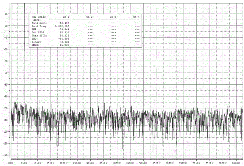
[0027] This patent implements a high-speed synchronous acquisition system with a 2-way sampling rate of 500MHz and a quantization bit width of 14bit through an FPGA-based high-speed acquisition circuit design. It achieves high synchronization, SNR and SFDR performance, and the board is designed based on FMC structure, which has wide applicability.

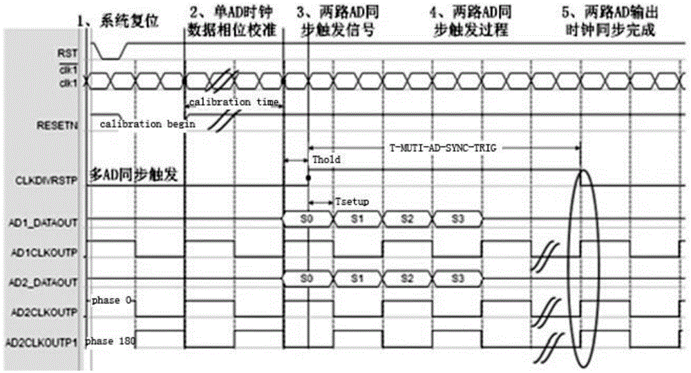
[0028] Such as figure 1 As shown, the design is based on multi-channel ultra-low jitter high-speed clock generation circuit, high-speed ADC front-end signal conditioning circuit, multi-channel ADC synchronization technology, high-speed ADC low-noise power supply design technology and layout technology, FPGA-based signal processing platform design technology, etc. , to complete the high-speed synchronous data acquisition of 2 broadband signals. The multi-channel high-speed synchronous clock circuit generates multiple low-j...


PUM


Abstract

The invention relates to a field programmable gate array (FPGA) based high-speed analog-digital converter (ADC) synchronous acquisition system, comprising an FPGA based signal processing platform and a high-speed ADC synchronous acquisition daughter board. A clock signal for ADC acquisition, a control signal and date collected by the ADC on the high-speed ADC synchronous acquisition daughter board are transmitted to the FPGA based signal processing platform, and the FPGA based signal processing platform performs subsequent signal processing; the high-speed ADC synchronous acquisition daughter board comprises an ultralow jitter synchronous clock generation circuit, a power supply module, and a plurality of high-speed ADC acquisition circuits; and the front end of each high-speed ADC acquisition circuit is connected with a broadband signal conditioning circuit. Synchronous sampling is performed on the ADC between different channels through a multichannel ADC synchronization technology; the ultralow jitter synchronous clock generation circuit generates multichannel low jitter clocks meeting high-speed ADC signal to noise ratio and synchronism requirements; due to adoption of the two-stage alternating current coupling broadband signal conditioning circuit, the high-speed ADC acquisition circuit can collect middle frequency signals with input frequency between 10kHz and 700MHz; and the power supply module adopts a low noise power supply design.

Description

technical field [0001] The invention belongs to the field of high-speed data acquisition, and specifically relates to an FPGA-based high-speed synchronous acquisition system. Background technique [0002] In the field of wireless communication and signal receiving and processing, the processed signal bandwidth is getting wider and wider, and the sampling rate of ADC is getting higher and higher. Specifications for A / D converters and D / A converters) and synchronicity and other performance indicators are increasingly demanding. The sampling rate of traditional signal acquisition boards is not high enough, and the SNR, SFDR and synchronization indicators cannot meet the requirements of broadband signal acquisition and processing, especially in the application of receiving equipment that requires synchronous processing of multi-channel signals. Can not meet the current mainstream design requirements, therefore, an urgent need for a high-performance new sampling technology. [...

Claims


Application Information

Patent Timeline
IPC IPC(8): H03M1/12H03M1/06
Inventor 秦艳召
Owner PANDA ELECTRONICS GROUP
Learn More