Embossed photovoltaic welding band and processing method thereof

A photovoltaic ribbon and embossing technology, applied in the field of solar energy, can solve the problems of special-shaped metal wires falling off, difficult to arrange parallel and twisted special-shaped metal wires, etc.

Active Publication Date: 2015-10-21
WENLING XUSHENG OPTOELECTRONICS TECH
View PDF5 Cites 6 Cited by
  • Summary
  • Abstract
  • Description
  • Claims
  • Application Information

AI Technical Summary

Problems solved by technology

[0004] Although the special-shaped metal wire is used in the above scheme to replace the process of embossing patterns on the surface of the ordinary photovoltaic ribbon to improve the welding strength of the back electrode of the crystalline silicon solar cell, the above-mentioned scheme has the following defects: First, the special-shaped metal wire is easy to fall off from the conductive base tape , especially in the process of handli

Method used


Image

  • Embossed photovoltaic welding band and processing method thereof
  • Embossed photovoltaic welding band and processing method thereof
  • Embossed photovoltaic welding band and processing method thereof

Examples


Embodiment Construction

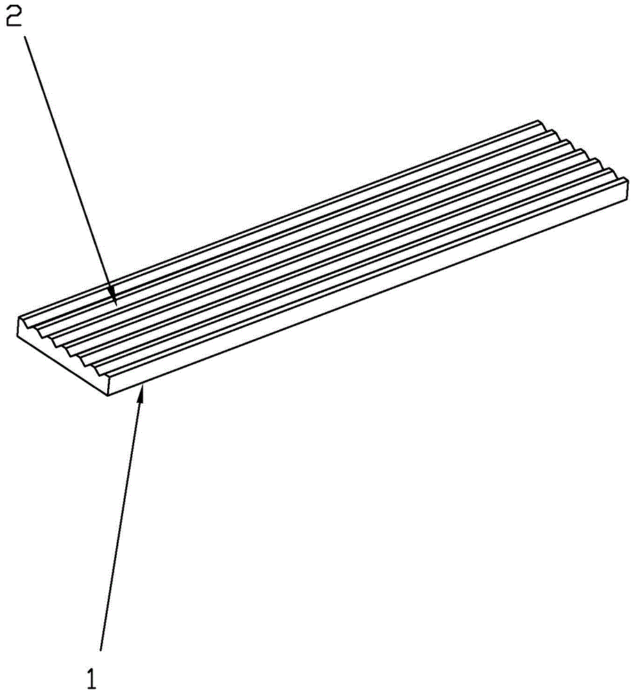
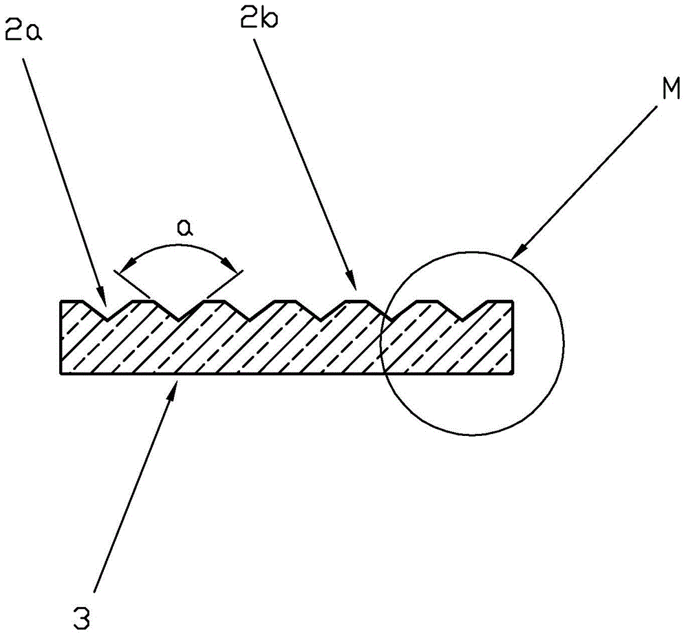
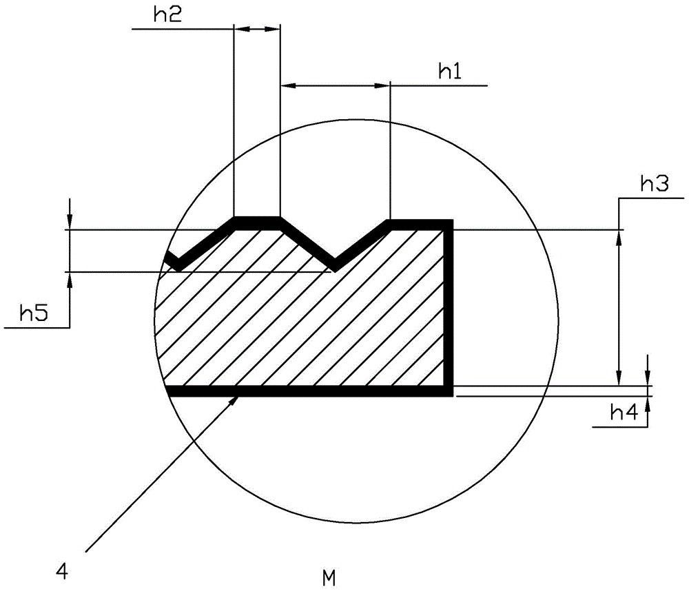
[0022] An embossed photovoltaic ribbon, comprising a conductive base tape 1, the conductive base tape 1 has a lower bonding surface 3 and an upper reflecting surface 2, the lower bonding surface 3 is a flat surface, and the upper reflecting surface 2 is distributed with reflecting grooves 2a, and the adjacent reflecting A coupling strip 2b is formed between the grooves 2a, the reflective groove 2a extends parallel to the length direction of the conductive base strip 1, the width h2 of the coupling strip is 0.2 to 0.4 times the width h1 of the top of the reflective groove, and the thickness h3 of the conductive base strip is 0.5mm- 1.0mm, and the depth h5 of the reflection groove is 0.1mm-0.2mm. If the width h2 of the coupling band is too large, it will affect the light reflected from the top of the reflective groove 2a, reducing the light utilization rate. If the width h2 of the coupling band is too small, there will be false welding and desoldering with the back electrode of t...


PUM

PropertyMeasurementUnit
Thicknessaaaaaaaaaa
Depthaaaaaaaaaa
Thicknessaaaaaaaaaa

Abstract

The invention discloses an embossed photovoltaic welding band and a processing method thereof. The embossed photovoltaic welding band includes a conducting base band having a lower adhering face and an upper reflecting face. The lower reflecting face is a flat face. Reflecting grooves are distributed in the upper reflecting face. Coupling bands are formed between the adjacent reflecting grooves. The embossed photovoltaic welding band is characterized in that the reflecting grooves extend in the length direction, being parallel to each other. The width of each coupling band is 0.2 to 0.4 times of the width of the top part of each reflecting groove. The thickness of the conducting base band is 0.5 to 1.0 mm. The depth of each reflecting groove is 0.1 to 0.2 mm. The invention also discloses a method for processing the above embossed photovoltaic welding band. By adopting the scheme, good incident light utilization rate can be achieved. Besides, good welding strength of the photovoltaic welding band and a back electrode of a crystalline silicon solar cell can be ensured.

Description

technical field [0001] The invention relates to an embossed photovoltaic welding ribbon and a processing method thereof, belonging to the technical field of solar energy. Background technique [0002] Photovoltaic ribbon is the key auxiliary material for connecting solar cells into strings. Solar cells are connected by ribbons to form a complete electrical path. Light energy is converted into electrical energy through solar cells, and the generated current forms a transmission circuit through ribbons, which provides Access basis. The base material of ordinary solder ribbon is copper, and the surface of the solder ribbon base material is coated with a tin layer. The entire ribbon surface is relatively flat. Although there are some special-shaped ribbons on the market at present, there are various regular grooves on the surface to achieve secondary reflection to reach the surface of the cell and be reused, thereby improving the utilization rate of incident light. [0003] Th...

Claims


Application Information

Patent Timeline
IPC IPC(8): H01L31/05
CPCY02E10/50H01L31/0512
Inventor 叶辉波
Owner WENLING XUSHENG OPTOELECTRONICS TECH
Why Eureka
Try Eureka