Method for machining MEMS resonant structure

A technology of resonant structure and processing method, applied in electrical components, impedance networks, etc., can solve the problems of high cost of SOI wafers and large investment in fixed assets of chip foundries, so as to reduce material costs, reduce production equipment costs, and reduce Effect of Temperature Coefficient of Frequency

Active Publication Date: 2015-10-21
GUANGDONG HEWEI INTEGRATED CIRCUIT TECH
View PDF5 Cites 6 Cited by
  • Summary
  • Abstract
  • Description
  • Claims
  • Application Information

AI Technical Summary

Problems solved by technology

[0006] The disadvantage of the above method is that: using SOI wafers, although the process is relatively simple, the cost of SOI wafers is very high
However, this special processing technology requires specific annealing equipment, including high temperature (generally greater than 1050°C) and special atmosphere (hydrogen or argon), which requires a large investment in fixed assets for chip foundries.

Method used


Image

  • Method for machining MEMS resonant structure
  • Method for machining MEMS resonant structure
  • Method for machining MEMS resonant structure

Examples


Embodiment Construction

[0065] The technical solutions of the present invention will be further described below in conjunction with the accompanying drawings and through specific implementation methods.

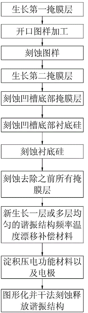
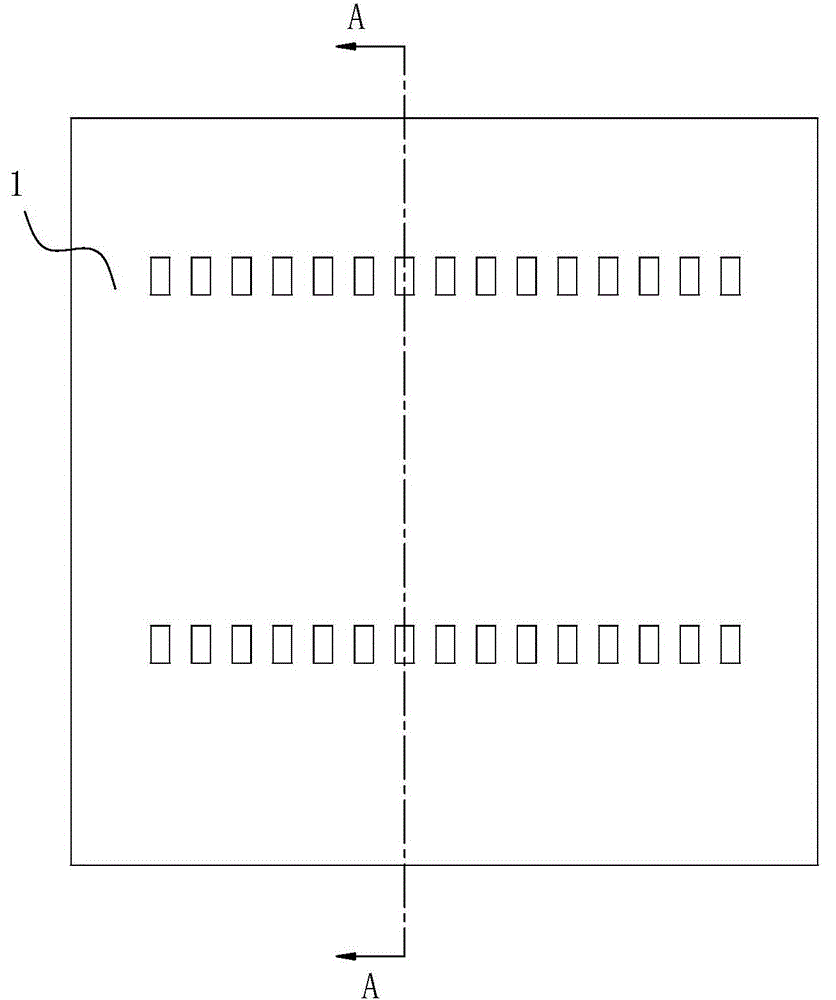
[0066] like Figure 1-13 Shown:

[0067] A processing method for a MEMS resonant structure, comprising the following steps:

[0068] Step S1, providing a silicon wafer as the substrate silicon 1, and growing a first mask layer 2 on the surface of the substrate silicon 1;

[0069] Step S2, processing an opening pattern on the first mask layer 2;

[0070] Step S3, removing the first mask layer 2 and the substrate silicon 1 corresponding to the opening pattern by dry etching, and forming a groove structure 4 on the substrate silicon 1;

[0071] Step S4, growing a second mask layer 3, forming a second mask layer 3 on the side walls and bottom of the groove of the groove structure 4, and forming a composite mask layer on the surface of the silicon substrate 1;

[0072] Step S5, removing the second ma...


PUM


Abstract

The invention discloses a method for machining an MEMS resonant structure. The method includes: providing silicon wafer as substrate silicon, and growing a first mask layer on the surface of the substrate silicon; machining open patterns on the first mask layer; removing parts of the first mask layer and the substrate silicon which are corresponding to the open patterns by dry etching, and forming groove structures on the substrate silicon; growing second mask layers, forming the second mask layers on groove side walls of the groove structures and the groove bottoms, and forming a composite mask layer on the surface of the substrate silicon; removing the second mask layers by dry etching, and completely removing the second mask layers of the groove bottoms; etching the substrate silicon again by dry etching, enabling the groove structures to be deepened, and enabling newly etched groove side walls not to be covered by mask layers; by wet etching, enabling the inside of the substrate silicon to be communicated with the open pattern to form a cavity; depositing lower electrodes, piezoelectric function materials and upper electrodes; and patterning and releasing the resonant structure by dry etching.

Description

technical field [0001] The invention relates to the technical field of semiconductor manufacturing, in particular to a method for processing a MEMS resonant structure, in particular to a method for simultaneously manufacturing resonant structures with different silicon film thicknesses on the same wafer. Background technique [0002] MEMS oscillator refers to a programmable oscillator produced by the micro-electromechanical system. It is an upgrade of the traditional quartz crystal oscillator. The shockproof effect is 25 times that of the former. It is not affected by vibration and is not fragile. features. [0003] The processing of the MEMS resonant structure in the prior art has the following methods: [0004] 1. Use the SOI wafer to oxidize its surface and then bond it to another substrate wafer with a pre-processed cavity. After the SOI wafer is thinned, the upper metal lower electrode, piezoelectric functional material and metal upper electrode are deposited respecti...

Claims


Application Information

Patent Timeline
Patent Type & Authority Applications(China)
IPC IPC(8): H03H9/24H03H3/007
Inventor 周志健陈磊邝国华
Owner GUANGDONG HEWEI INTEGRATED CIRCUIT TECH
Why Eureka
Try Eureka