Chip packaging structure with package and realization process

A technology of chip packaging structure and packaging structure, which is applied in the direction of electrical components, electric solid devices, circuits, etc., can solve problems such as delamination damage, moisture absorption, etc., and achieve the effect of improving protection level, product yield rate, and reliability

Inactive Publication Date: 2015-10-28
BEIJING UNIV OF TECH
View PDF4 Cites 4 Cited by
  • Summary
  • Abstract
  • Description
  • Claims
  • Application Information

AI Technical Summary

Problems solved by technology

After being separated into a single chip, the sidewall and bottom of the silicon are exposed, so that it is in direct contact with the outside world, which may absorb moisture, delaminate or be damaged in other ways, causing some reliability problems

Method used


Image

  • Chip packaging structure with package and realization process
  • Chip packaging structure with package and realization process

Examples


Embodiment Construction

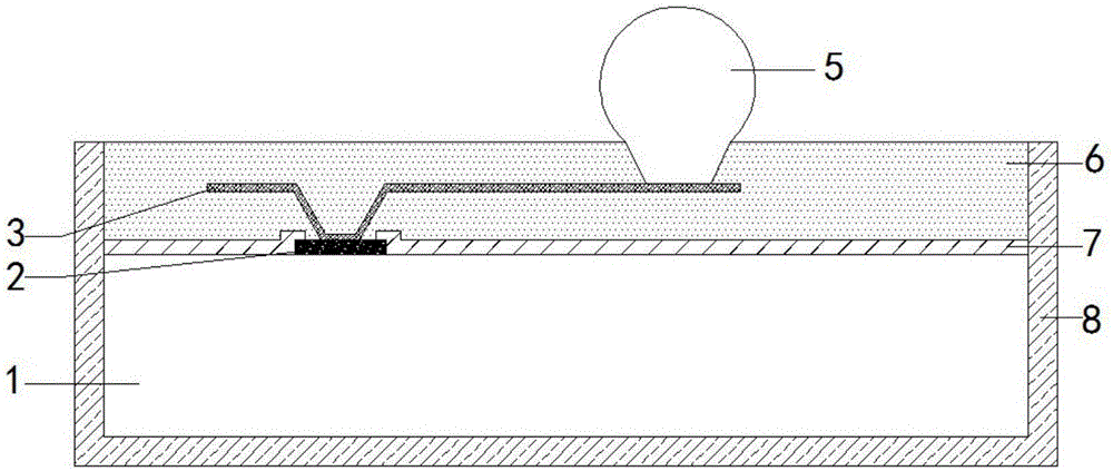
[0031] The present invention proposes a chip packaging structure with encapsulation and its realization process, such as figure 1 As shown, the packaging structure includes a chip unit (9) and a first insulating layer (6) and a second insulating layer (8) covering the chip unit, and the bottom and both sides of the chip unit (9) are covered by the second insulating layer (8). ) package, the top of the chip unit (9) is wrapped by the first insulating layer (6); the chip unit (9) includes a silicon chip (1) and an oxide layer (7) containing an integrated circuit function layer, and contains an integrated circuit function The silicon wafer (1) of the first layer is located below the chip unit (9); the oxide layer (7) is placed above the silicon wafer (1) containing the integrated circuit function layer; there are several PINs in the oxide layer (7) Pin (2), the PIN pin (2) is a metal pin.

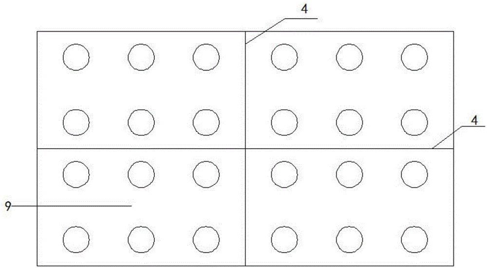
[0032] Such as Figure 1~2 As shown, the process flow for forming a six-sided covering s...


PUM


Abstract

The invention provides a chip packaging structure with a package and a realization process. The process includes following steps: providing a wafer; thinning the backside of the wafer; leading out a line on a function surface of the wafer after film-turning and forming a metal wiring layer; coating an insulating layer on the line layer; etching a ball-implanting pad on the insulating layer and implanting a soldering ball; cutting the wafer after film-turning; covering an insulating layer on the backside of the wafer and filling a cutting channel; and cutting and separating the wafer into single chips and forming a six-surface wrapping structure. According to the chip packaging structure with the package, adverse influences on silicon in a product production process, such as moisture absorption, layering, or other damages can be improved, the chip protection grade is improved, the influence of the CTE gap of packaging materials on the chips is reduced, the reliability of the product is improved, and the product yield rate is increased.

Description

technical field [0001] The invention relates to a wafer-level chip size packaging process method for a semiconductor chip, in particular to a chip packaging structure with encapsulation and a realization process. technical background [0002] Wafer-level chip size packaging means that after the entire wafer is packaged, the wafer is cut into individual chips. After being separated into a single chip, the sidewall and bottom of the silicon are exposed, so that it is in direct contact with the outside world, which may absorb moisture, delaminate or be damaged in other ways, causing some reliability problems. Contents of the invention [0003] In order to improve the protection level of the chip, prevent the erosion of external substances, and reduce the impact of the CTE gap of the encapsulation material on the chip, the present invention provides a chip encapsulation structure and implementation process with encapsulation. [0004] A chip packaging structure with encapsula...

Claims


Application Information

Patent Timeline
Patent Type & Authority Applications(China)
IPC IPC(8): H01L23/31H01L21/56
CPCH01L2224/11
Inventor 秦飞别晓锐史戈安彤武伟肖智轶
Owner BEIJING UNIV OF TECH
Why Eureka
Try Eureka