LED packaging structure and manufacturing method thereof

A technology of LED packaging and manufacturing methods, which is applied in the direction of electrical components, circuits, semiconductor devices, etc., can solve problems such as voids, poor contact, and manufacturing bottlenecks, and achieve the effects of good gap controllability, simple process steps, and reduced manufacturing costs

Active Publication Date: 2015-10-28
HONGLI ZHIHUI GRP CO LTD
View PDF3 Cites 16 Cited by
  • Summary
  • Abstract
  • Description
  • Claims
  • Application Information

AI Technical Summary

Problems solved by technology

In this way, during the heating process, the fluorescent adhesive layer will expand due to heat, which will cause unevenness between the fluorescent adhesive layer and the bottom of the chip, which will lead to poor contact, voids or even non-contact phenomena when the chip and the pad on the substrate are bonded, affecting the connection between the chip and the substrate. Reliability of substrate electrical connection
[0007] In view of the above technical problems, the inventor utilizes the special structure of the flip chip. The inventor believes that if the electrodes of the flip chip and the encapsulant form a step, the above technical problem may be solved. However, when manufacturing the package level chip, the encapsulation adhesive It is fluid before curing, so it is difficult to form a step between the electrode and the encapsulant during the encapsulation process, causing a large bottleneck in manufacturing

Method used


Image

  • LED packaging structure and manufacturing method thereof
  • LED packaging structure and manufacturing method thereof
  • LED packaging structure and manufacturing method thereof

Examples


Embodiment 1

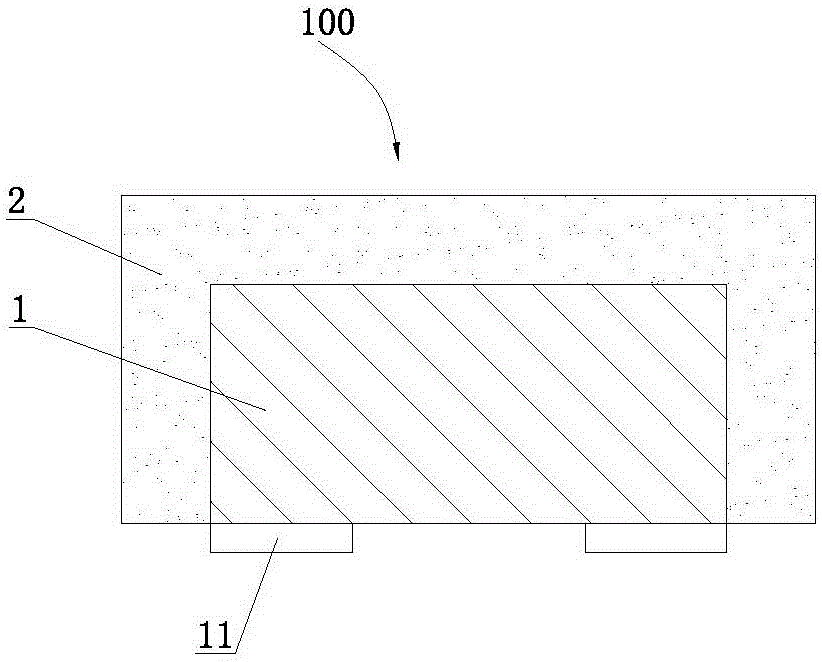
[0046] like figure 1 As shown, the LED packaging structure 100 includes a flip chip 1, the flip chip 1 includes a flip chip body and an electrode 11, the electrode 11 is arranged at the bottom of the flip chip body, and the electrode 11 protrudes from the bottom surface of the flip chip body. The side surface and the top surface of the flip chip body are coated with encapsulation glue 2, and the encapsulation glue 2 is fluorescent glue. The lower surface of the encapsulant 2 is higher than the lower surface of the electrode 11 . In this embodiment, the lower surface of the encapsulant 2 is flush with the lower surface of the flip chip body.

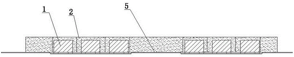
[0047] like figure 2 As shown, since the lower surface of the encapsulant 2 is higher than the lower surface of the electrode 11, in the process of fixing the LED package structure 100 to the substrate 3, a space is formed between the lower surface of the encapsulant 2 and the substrate 3, so even if the encapsulation The glue 2 has d...

Embodiment 2

[0049] like figure 2 As shown, the LED device includes an LED packaging structure 100 and a substrate 3 .

[0050] The LED packaging structure 100 includes a flip chip 1, the flip chip 1 includes a flip chip body and electrodes 11, the electrodes 11 are arranged at the bottom of the flip chip body, and the electrodes 11 protrude from the bottom surface of the flip chip body. The side surface and the top surface of the flip chip body are coated with encapsulation glue 2, and the encapsulation glue 2 is fluorescent glue. The lower surface of the encapsulant 2 is higher than the lower surface of the electrode 11 . In this embodiment, the lower surface of the encapsulant 2 is flush with the lower surface of the flip chip body.

[0051] like figure 2As shown, since the lower surface of the encapsulant 2 is higher than the lower surface of the electrode 11, in the process of fixing the LED package structure 100 to the substrate 3, a space is formed between the lower surface of ...

Embodiment 3

[0053] The method for manufacturing the LED package structure of the above-mentioned embodiment 1 is:

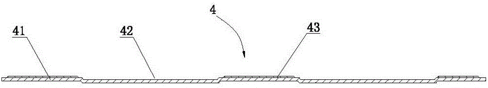
[0054] (1) if image 3 As shown, a stage 4 is provided, and the stage 4 includes a carrier plate 41 with more than one concave cavity 42 on the carrier plate 41 . The side surface of the recessed cavity 42 is an inclined surface extending from top to bottom toward the interior of the recessed cavity 42 , so that the gap between the encapsulant 2 and the bottom surface of the recessed cavity 42 is uniform and the gap is controllable.

[0055] (2) if Figure 4 As shown, the isolation film 5 is laid on the stage 4, and the isolation film 5 is attached to the carrier plate 41, the bottom surface of the recessed cavity 42 and the side of the recessed cavity 42; in this embodiment, the isolation film is made of UV film.

[0056] (3) if Figure 5 As shown, the flip chip 1 is fixed in the recessed cavity 42 on the isolation film 5; the electrode 11 of the flip chip 1 is connected...


PUM


Abstract

The invention discloses an LED packaging structure and a manufacturing method thereof. The manufacturing method comprises the steps of providing a carrier on which concave cavities are formed, laying an isolation film on the carrier, fixing flip chips in the concave cavities, and carrying out glue injection, curing, cutting and separation. The LED packaging structure comprises a flip chip which is provided with electrodes at the bottom, the sides and top of the flip chip are coated with packaging adhesive, and the lower surface of the packaging adhesive is higher than the lower surfaces of the electrodes. By adopting the manufacturing method, an LED packaging structure with a step between each electrode and the packaging adhesive can be manufactured. The void ratio of connection between the LED packaging structure and a substrate is reduced, the reliability of LED packaging structure fixing is improved, and the reliability of electrical connection between the LED packaging structure and the substrate is improved.

Description

technical field [0001] The invention relates to an LED packaging structure and a manufacturing method. Background technique [0002] The traditional packaging of LED is to fix the chip on the substrate first, and then implement the packaging process on the chip on the substrate. The LED device formed by this packaging process, on the one hand, the chip may move during the packaging process, causing The position accuracy of the chip package is not high, and it will also affect the conductivity of the chip and the substrate. On the other hand, the thickness uniformity of the package glue is difficult to control, resulting in a larger volume and weight of the LED device, which also has a certain effect on light output. Influence. For LED devices with multiple chips packaged on the same substrate, such as COB light sources, etc., once the package is completed and the packaged chips are determined, if the chip consistency is not good or some chips are damaged, it will affect Th...

Claims


Application Information

Patent Timeline
Patent Type & Authority Applications(China)
IPC IPC(8): H01L33/54H01L33/62
CPCH01L33/54H01L33/62
Inventor 熊毅杜金晟郭生树朱富斌李坤锥
Owner HONGLI ZHIHUI GRP CO LTD
Why Eureka
Try Eureka