Supercharge Your Innovation With Domain-Expert AI Agents!

Method of manufacturing LED laminated circuit board based on inorganic substance

A manufacturing method and circuit board technology, which is applied to circuits, electrical components, semiconductor devices, etc., can solve problems such as inability to guarantee performance consistency, cumbersome bonding process, and hidden dangers of product stability and reliability.

Active Publication Date: 2015-11-04
ADVANCED DIGITAL DISPLAY WUXI CO LTD
View PDF4 Cites 1 Cited by
  • Summary
  • Abstract
  • Description
  • Claims
  • Application Information

AI Technical Summary

Problems solved by technology

[0003] However, when the traditional circuit board is used as the LED circuit substrate, the impurities, pores, thermal stress, thermal expansion and other defects in the material will cause fatal hidden dangers to product stability and reliability.
Moreover, when the resolution of the semiconductor display is increased to a certain extent (for example, when the pixel pitch is required to be less than 1MM), the processing cannot be realized.
Therefore, traditional circuit boards are completely unable to meet the requirements of small size and high precision.
At the same time, the subsequent bonding process with LEDs is cumbersome, and the consistency of performance among multiple LED chips carried by an LED circuit substrate cannot be guaranteed, which may affect the performance of the final product

Method used


Image

  • Method of manufacturing LED laminated circuit board based on inorganic substance
  • Method of manufacturing LED laminated circuit board based on inorganic substance
  • Method of manufacturing LED laminated circuit board based on inorganic substance

Examples


preparation example Construction

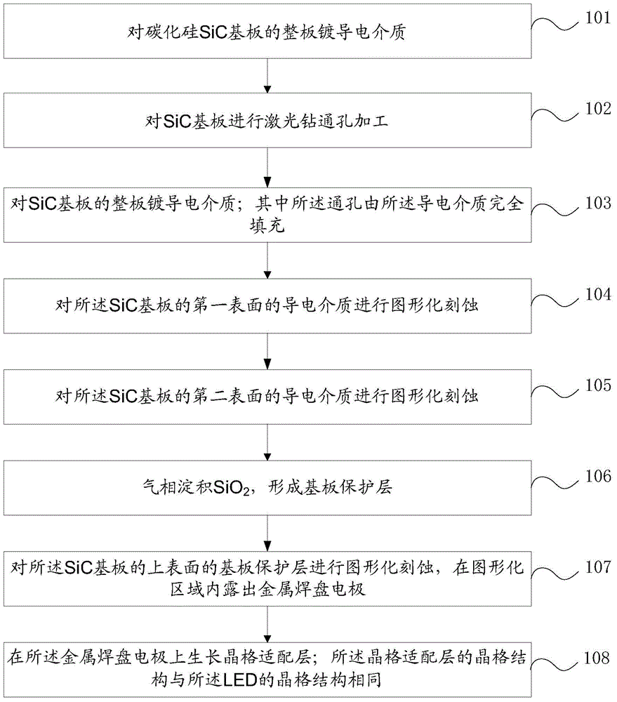
[0067] The preparation method of the above step 101-step 108 provides a method for preparing a single-layer LED substrate. If a multi-layer substrate is to be prepared, the following steps can be performed before the above step 106:

[0068] 1) Vapor deposition of SiC to form the filling layer of the patterned etching area and the surface insulating layer of the SiC substrate;

[0069] 2) performing patterned etching on the surface insulating layer of the SiC substrate, and etching until the conductive medium is exposed in the patterned area;

[0070] 3) Plating a conductive medium on the entire board of the SiC substrate;

[0071] 4) performing patterned etching on the conductive medium on the first surface of the SiC substrate;

[0072] 5) Perform patterned etching on the conductive medium on the second surface of the SiC substrate.

[0073] The above steps 1)-5) can be repeated multiple times according to the required number of substrate layers.

[0074] The method for m...


PUM

PropertyMeasurementUnit
thicknessaaaaaaaaaa
thicknessaaaaaaaaaa
thicknessaaaaaaaaaa

Abstract

The invention relates to a method of manufacturing an LED laminated circuit board based on inorganic substances, comprising the steps of: plating conductive media on an entire SiC substrate; performing through hole laser drilling processing on the SiC substrate, wherein through holes are completely filled by the conductive media; performing graphical etching on the conductive media on the first surface of the SiC substrate; performing graphical etching on the conductive media on the second surface of the SiC substrate; gas plating SiO2 to form substrate protective layers; performing graphical etching on the substrate protective layer on the upper surface of the SiC substrate, and exposing metal welding plate electrodes to graphical areas; and growing lattice adaptation layers on the metal welding plate electrodes, wherein lattice structures of the lattice adaptation layers are same with LED lattice structures.

Description

technical field [0001] The invention relates to the field of semiconductors, in particular to a method for manufacturing an inorganic-based LED laminated circuit board. Background technique [0002] With the development of traditional semiconductor display products to this day, supporting or cross-industry resources have been greatly enriched and perfected. In the traditional LED product structure, FR4 circuit boards are usually used as LED circuit substrates. [0003] However, when the traditional circuit board is used as the LED circuit substrate, the impurities, pores, thermal stress, thermal expansion and other defects in the material will cause fatal hidden dangers to product stability and reliability. Moreover, when the resolution of the semiconductor display is increased to a certain extent (for example, when the pixel pitch is required to be less than 1MM), the processing cannot be realized. Therefore, traditional circuit boards are completely unable to meet the re...

Claims


Application Information

Patent Timeline
Patent Type & Authority Applications(China)
IPC IPC(8): H01L33/48H01L33/62
Inventor 程君严敏周鸣波
Owner ADVANCED DIGITAL DISPLAY WUXI CO LTD
Features
  • R&D
  • Intellectual Property
  • Life Sciences
  • Materials
  • Tech Scout
  • Unparalleled Data Quality
  • Higher Quality Content
  • 60% Fewer Hallucinations
Learn More