Touch screen display apparatus and manufacturing method thereof

A technology for display devices and touch screens, applied to instruments, electrical digital data processing, and input/output processes of data processing, etc., can solve problems such as fragile screens, increased size of electronic equipment, uneven light transmittance, etc., to reduce assembly Difficulty, reducing the thickness of the screen, and increasing the effect of interactive experience

Active Publication Date: 2015-11-18
BEIJING SOGOU INTELLIGENT TECH CO LTD
View PDF5 Cites 5 Cited by
  • Summary
  • Abstract
  • Description
  • Claims
  • Application Information

AI Technical Summary

Problems solved by technology

[0004] The above touch screen technologies have their own advantages and disadvantages, but for some specific operators, such as children, there are corresponding problems: First, the resistive touch technology needs to set a layer of soft touch-sensitive piezoelectric on the outer surface of the screen display area. Thin film, this layer of medium is not wear-resistant, and children often do not notice the protection of the screen, which is easy to damage the screen; at the same time, resistive touch technology can only be applied to flat screen surfaces, not curved screen surfaces , so resistive touch cannot be realized on a more rounded touch screen designed for children; second, the capacitive touch technology is seriously reflective, and the four-layer composite touch screen of capacitive technology has uneven light transmittance for each wavelength of light, and there is color distortion Due to the reflection of light between the layers, the image characters are blurred; third, the copper foil of the copper foil touch screen technology increases the thickness of the screen, which increases the size of the electronic device and increases the size of the electronic device. Assembly Difficulty

Method used


Image

  • Touch screen display apparatus and manufacturing method thereof
  • Touch screen display apparatus and manufacturing method thereof
  • Touch screen display apparatus and manufacturing method thereof

Examples


Embodiment 1

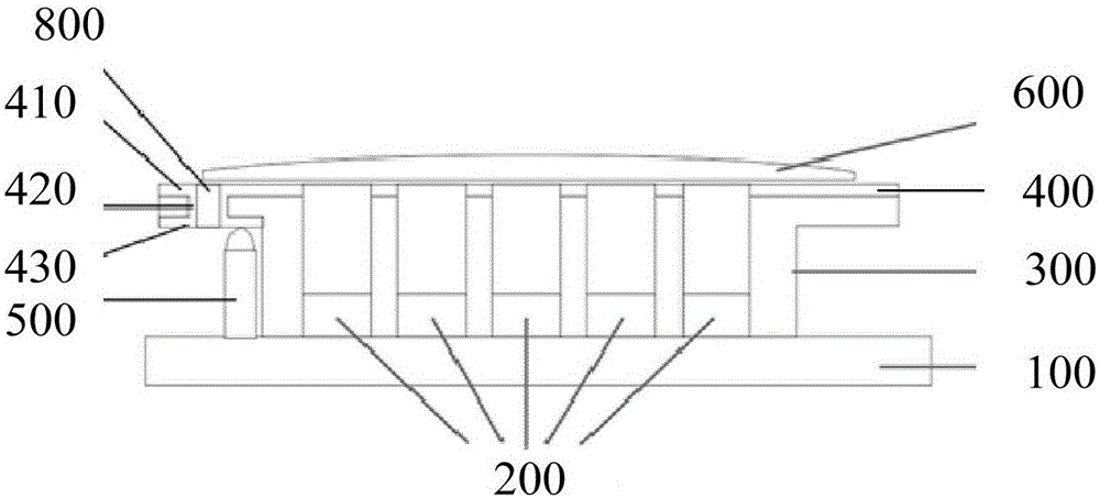
[0058] refer to figure 1 , shows a schematic cross-sectional structure diagram of a touch screen display device according to an embodiment of the present invention, referring to Figure 2a , Figure 2b A schematic diagram of the axonometric structure of a touch screen display device according to an embodiment of the present invention is shown respectively. Specifically, the touch screen display device may include the following units:

[0059] motherboard 100;

[0060] An LED light source 200 located on the main board 100;

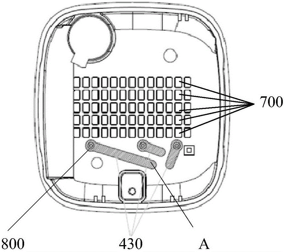
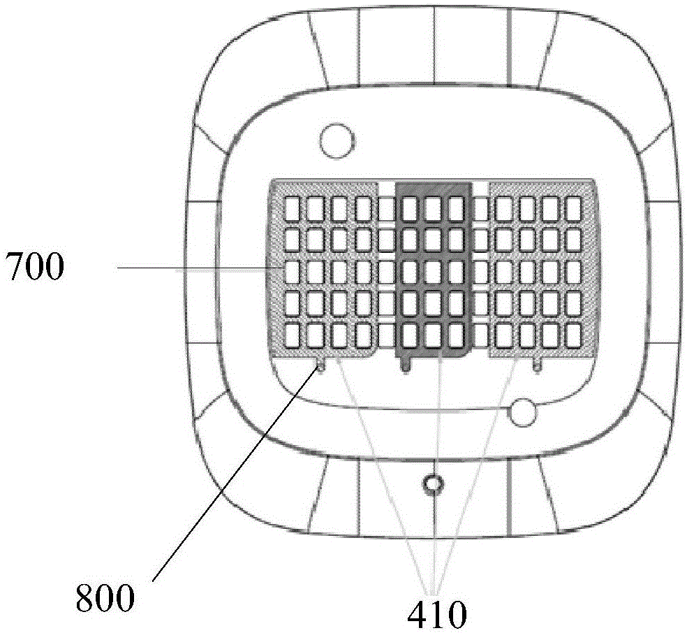
[0061] The shading plate 300 located on the upper part of the main board 100; the shading plate 300 is provided with a hole structure at a position corresponding to the LED light source 200;

[0062] Laser engraving the induction metal layer 400 on the surface of the light shielding plate 300; wherein, a metal connection is formed between the induction metal layer and the main board; and

[0063] The touch layer 600 located on the upper part of the ligh...


PUM


Abstract

Embodiments of the present invention provide a touch screen display apparatus and a manufacturing method thereof. The touch screen display apparatus specifically comprises: a main board; an LED light source located above the main board; a shading plate located above the main board; a porous structure arranged on a position that is on the shading plate and corresponds to the LED light source; an induction metal layer that is laser-etched on a surface of the shading plate, wherein a metal connection is formed between the induction metal layer and the main board; and a touch layer located above the shading plate. According to the touch screen display apparatus and the manufacturing method thereof, a screen thickness and a size of an electronic device can be reduced, and assembly difficulty of the touch screen display apparatus can be reduced.

Description

technical field [0001] The present invention relates to the technical field of touch display, in particular to a touch screen display device and a manufacturing method of the touch screen display device. Background technique [0002] Electronic equipment technology has developed rapidly in recent years, and people are increasingly inseparable from the use of electronic equipment in their work and life. Existing electronic equipment generally has a touch screen, and users can use their fingers to manipulate the electronic equipment flexibly and conveniently on the touch screen. Therefore, the quality of the touch screen directly affects the user experience. [0003] At present, the commonly used touch screen technologies in the industry mainly include: resistive touch screen technology, capacitive touch screen technology and copper skin touch screen structure; among them, resistive touch technology uses two layers of highly transparent conductive layers to form a touch screen...

Claims


Application Information

Patent Timeline
Patent Type & Authority Applications(China)
IPC IPC(8): G06F3/041
Inventor 肖子秋
Owner BEIJING SOGOU INTELLIGENT TECH CO LTD
Why Eureka
Try Eureka