Preparation method for trapezoid pixel Bank structure and OLED device

A trapezoidal, pixel technology, applied in semiconductor/solid-state device manufacturing, electric solid-state devices, semiconductor devices, etc., can solve problems such as difficult surface hydrophilic and hydrophobic treatment of vertical pixel Bank structure, poor device pixel uniformity, and reduced device aperture ratio, etc. Achieve the effect of reducing the impact of lateral erosion, avoiding device open circuits, and reducing device fabrication costs

Active Publication Date: 2015-11-18
GUANGDONG JUHUA PRINTING DISPLAY TECH CO LTD
View PDF5 Cites 14 Cited by
  • Summary
  • Abstract
  • Description
  • Claims
  • Application Information

AI Technical Summary

Problems solved by technology

[0008] The purpose of the present invention is to provide a method for preparing a trapezoidal pixel Bank structure, aiming to solve the poor uniformity of device pixels caused by the trapezoidal pixel Bank structure produced by the existing vertical exposure method, and even lead to device open circuit, reduce the device aperture ratio, or vertical The pixel bank structure is difficult to carry out surface hydrophilic and hydrophobic treatment, which is not conducive to the problem of solution method for making OLED devices

Method used


Image

  • Preparation method for trapezoid pixel Bank structure and OLED device
  • Preparation method for trapezoid pixel Bank structure and OLED device
  • Preparation method for trapezoid pixel Bank structure and OLED device

Examples


Embodiment Construction

[0033] In order to make the technical problems, technical solutions and beneficial effects to be solved by the present invention clearer, the present invention will be further described in detail below in conjunction with the accompanying drawings and embodiments. It should be understood that the specific embodiments described here are only used to explain the present invention, not to limit the present invention.

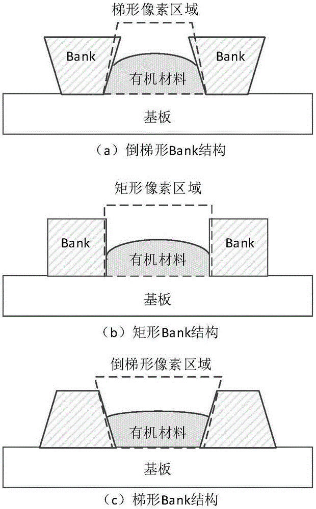
[0034] combined with Figure 2-7 , the embodiment of the present invention provides a method for preparing a trapezoidal pixel Bank structure, comprising the following steps:

[0035] S01. Provide a TFT backplane, coat a layer of Bank material on the electrodes of the TFT backplane, and bake the Bank material to form a Bank layer with adhesion to the electrodes, wherein the Bank material is negative bank material;

[0036]In the above step S01, the TFT backplane includes a TFT array and electrodes sequentially stacked on a hard carrier substrate. As a preferred ...


PUM


Abstract

The invention is applicable to the printing and displaying technology field and provides a preparation method for a trapezoid pixel Bank structure and an OLED device. The preparation method for the trapezoid pixel Bank structure comprises steps of providing a TFT backboard, preparing a Bank layer on the electrode of the TFT backboard, performing two times of exposure, development and etching on the Bank layer to form an inverted trapezoid pixel area, and obtaining a trapezoid pixel Bank structure having the trapezoid Bank. The preparation method for the trapezoid pixel Bank can effectively compensate the transverse corrosion for the pixel Bank by the developing liquid and corrosive liquid so as to obtain a trapezoid pixel Bank structure having an inclination angle of Alpha, overcome the affect on the uniformity of the member pixel caused by the over-etching on the bottom of the Bank, avoid the member open circuit and reduce the aperture opening ratio of the member.

Description

technical field [0001] The invention belongs to the technical field of printing and display, and in particular relates to a trapezoidal pixel Bank structure and a preparation method of an OLED device. Background technique [0002] OLED display devices are considered to be the next-generation flat-panel display emerging application technology due to their advantages of self-illumination, no need for backlight, high contrast, thin thickness, wide viewing angle, fast response speed, and flexible panels. At present, for the preparation of OLED display devices, vacuum evaporation and printing technologies are usually used to prepare, which is the current international mainstream development technology. The vacuum evaporation technology of small molecules is relatively mature and has been industrialized at present, and small and medium-sized full-color display screens have been launched in batches, which are applied in the fields of electronic equipment such as MP3, MP4, mobile ph...

Claims


Application Information

Patent Timeline
Patent Type & Authority Applications(China)
IPC IPC(8): H01L21/027H01L27/32H01L51/56
CPCH01L21/0274H10K71/00
Inventor 高卓李耘
Owner GUANGDONG JUHUA PRINTING DISPLAY TECH CO LTD
Why Eureka
Try Eureka