Display substrate and manufacturing method thereof, display device, and mask plate

A technology for display substrates and manufacturing methods, applied in the fields of masks, display substrates and their manufacture, and display devices, capable of solving the problems of low resolution of display substrates

Inactive Publication Date: 2015-11-18
BOE TECH GRP CO LTD +1
View PDF0 Cites 11 Cited by
  • Summary
  • Abstract
  • Description
  • Claims
  • Application Information

AI Technical Summary

Problems solved by technology

[0005] In order to solve the problem of low resolution of the display substrate in the prior art, the present invention provides a display substrate and a manufacturing method thereof, a display device, and a mask

Method used


Image

  • Display substrate and manufacturing method thereof, display device, and mask plate
  • Display substrate and manufacturing method thereof, display device, and mask plate
  • Display substrate and manufacturing method thereof, display device, and mask plate

Examples


Embodiment Construction

[0118] In order to make the object, technical solution and advantages of the present invention clearer, the present invention will be further described in detail below in conjunction with the accompanying drawings. Obviously, the described embodiments are only some embodiments of the present invention, rather than all embodiments . Based on the embodiments of the present invention, all other embodiments obtained by persons of ordinary skill in the art without making creative efforts belong to the protection scope of the present invention.

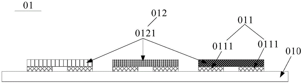
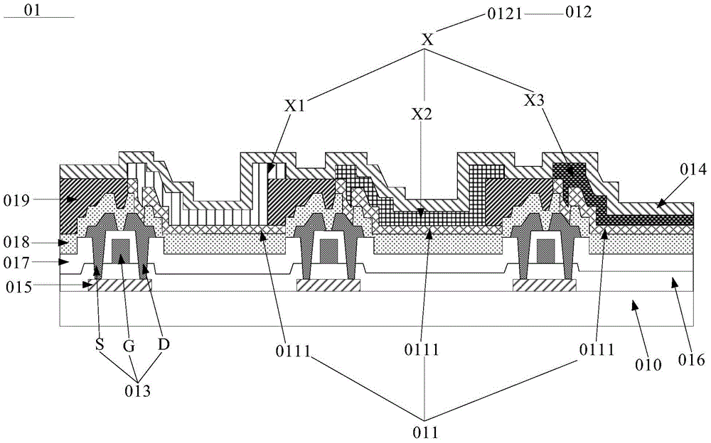
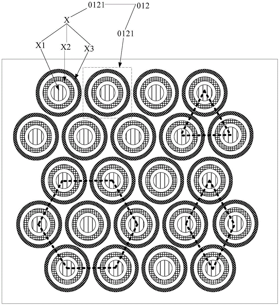
[0119] Please refer to figure 1 , which shows a schematic structural diagram of a display substrate 01 provided by an embodiment of the present invention. see figure 1 , the display substrate 01 includes: a base substrate 010, the base substrate 010 may be a transparent substrate, specifically, it may be a substrate made of light-guiding and non-metallic materials with certain firmness such as glass, quartz, and transparent resin.

[012...


PUM


Abstract

The invention discloses a display substrate and a manufacturing method thereof, a display device, and a mask plate, belonging to the technical field of display. The display substrate comprises a base substrate, an anode layer is formed on the base substrate, and the anode layer includes multiple anode structures. A pixel arrangement structure is formed on the base substrate with the anode layer. The pixel arrangement structure includes multiple pixels. Each pixel includes at least three sub pixels. Each sub pixel corresponds to at least two anode structures, the at least two anode structures corresponding to the same sub pixel do not contact, and each of the at least two anode structures corresponding to the same sub pixel is used to drive part of the same sub pixel to emit light. The problem that the resolution of the display substrate in the prior art is low is solved, and an effect of display substrate resolution improvement is achieved. The display substrate and the manufacturing method thereof, the display device, and the mask plate are used in the field of display.

Description

technical field [0001] The invention relates to the field of display technology, in particular to a display substrate, a manufacturing method thereof, a display device, and a mask. Background technique [0002] An organic light-emitting diode (English: Organic Light-Emitting Diode; abbreviation: OLED) display device is a display device with an autonomous light emitting function. The OLED display device includes a plurality of pixels arranged in a matrix, and the OLED display device can be divided into an active matrix organic light emitting diode (English: ActiveMatrix / OrganicLightEmittingDiode; abbreviation: AMOLED) display device and a passive matrix organic light emitting diode (OLED) according to the driving method of its pixels. Light-emitting diode (English: PassivematrixOrganicLight-EmittingDiode; abbreviation: PMOLED) display device, among which, AMOLED display device is characterized by its thin thickness, light weight, active light emission, fast response, wide vie...

Claims


Application Information

Patent Timeline
Patent Type & Authority Applications(China)
IPC IPC(8): H01L27/32H01L21/77G02F1/015G03F7/20G03F1/00
CPCC23C14/042H10K59/35H10K59/352H10K59/353
Inventor 张伟吴永凯孙乐任艳伟赵艳艳张琨鹏王晓康
Owner BOE TECH GRP CO LTD
Why Eureka
Try Eureka