Etching Compensation Method for High Precision Packaging Substrate

A technology of packaging substrate and compensation method, which is applied in the direction of lithography/pattern, pattern and lithography, printed circuit, etc., can solve the problems of poor line width accuracy/spacing ability, poor line width tolerance control ability, and improper definition of isolated lines and other issues, to achieve the effect of good line width quality, strong graphic adhesion, and good graphic accuracy

Active Publication Date: 2018-10-02
NAT CENT FOR ADVANCED PACKAGING
View PDF4 Cites 0 Cited by
  • Summary
  • Abstract
  • Description
  • Claims
  • Application Information

AI Technical Summary

Problems solved by technology

[0004] 1. There are large differences in the etching of different structural patterns, and the line width tolerance control ability is poor. The compromise compensation value is limited by the minimum spacing, and choosing a larger compensation value leads to poor line width accuracy / spacing capability;
[0005] 2. For isolated lines (judgment principle: there is no conductor copper design within 50mm on both sides of the wire) manual selection and more compensation; it is easy to miss and make mistakes, and the definition of isolated lines is improper, which will not achieve the effect

Method used


Image

  • Etching Compensation Method for High Precision Packaging Substrate
  • Etching Compensation Method for High Precision Packaging Substrate
  • Etching Compensation Method for High Precision Packaging Substrate

Examples


Embodiment Construction

[0025] The present invention will be further described below in conjunction with drawings and embodiments.

[0026] Such as Figure 1~6 Shown, the steps of the present invention are as follows:

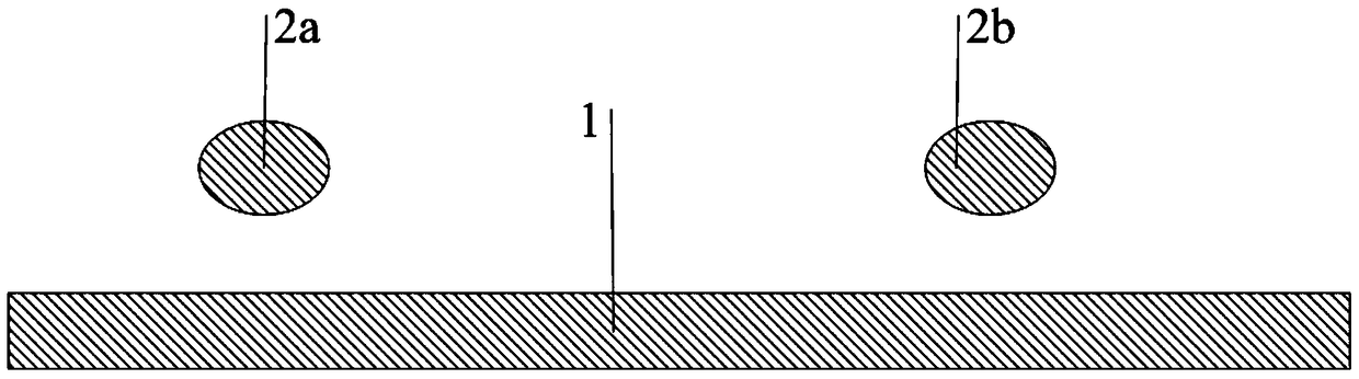
[0027] The first step: graph classification.

[0028] According to the layout design of the substrate, all design graphic elements are classified, and the graphic types include wires, pads, vias, heat dissipation copper surfaces, etc. Such as figure 1 As shown, the graphic elements are divided into wire 1, pad 2a, 2b.

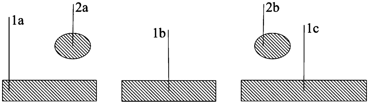
[0029] Step 2: Break the wire into multiple segments.

[0030] According to the design logic of adjacent graphics, break all wires into multiple segments, that is, one wire can be broken into 3 segments, 4 segments, etc., such as figure 2 As shown, the wire 1 is broken into three segments, respectively 1a, 1b, and 1c. Considering the adjacent graphics, one line will be broken into multiple line segments. At this time, it should be adjusted according to the design...


PUM


Abstract

The invention relates to an etching compensation method suitable for a high-precision packaging substrate. The method includes the steps: classifying all design graphic elements according to classification of graphs on the basis of the layout design of a substrate; breaking all leads into segments on the basis of design logic of the adjacent graphs; calculating the optimum compensation value for graphs designed on the same layer according to the types and intervals of the graphs; correcting according to the minimum interval and determining a compensation value after correction; compensating for each type of graphs through the corrected compensation value: symmetrically compensating for a spherical array pad and a binding pad, compensating for both sides of a lead, and compensating for four sides of a surface mount pad; and finally conducting minimum interval analysis inspection for the layered graphs that undergo dynamic compensation, and determining a compensation result. The design scheme utilizing partition dynamic etching compensation is adopted, the graph precision and the signal transmission precision of the whole packaging substrate are improved, the machining cost is reduced, and the graph precision of the packaging substrate and the reliability of subsequent packaging are also improved.

Description

technical field [0001] The invention relates to an etching compensation method for a high-precision packaging substrate, which belongs to the technical field of advanced microelectronic packaging. Background technique [0002] With the rapid development of electronic technology, the requirements for circuit boards are getting higher and higher, especially for packaging substrates. For high precision, high density, and the requirements for impedance control and line width tolerance of the outer layer of the packaging substrate are becoming more and more stringent. Therefore, it is necessary to have stable and uniform processing capacity for etching equipment. However, for high-density, high-precision packaging substrates, conventional etching compensation methods are difficult to meet the line width accuracy requirements of rapidly developing dense lines and isolated lines, and there will be different areas, different types of lines, and finished graphic sizes of different ty...

Claims


Application Information

Patent Timeline
Patent Type & Authority Patents(China)
IPC IPC(8): H05K3/00
CPCH05K3/0017H05K2203/0502
Inventor 宋阳
Owner NAT CENT FOR ADVANCED PACKAGING
Why Eureka
Try Eureka